

KIT33905D5EKEVBE主要特性,建立框图,电路图,和PCB元件
汽车电子
描述
Freescale公司的MC33903/4/5是第二代的系统基础芯片(SBC),能作为MCU的先进电源管理,并集成了几种先进的集成电路如传感器和CAN收发器,内置了增强高速CAN接口(ISO11898-2和-5),以及本地和总线故障诊断,保护与故障安全操作模式.主要用在航空和水下系统,汽车和机器人系统,农场设备,灯和电感负载控制,DC马达控制,工业激励控制等.本文介绍了MC33903/4/5系列产品主要特性,框图和简化应用框图,评估板KIT33905D5EKEVBE主要特性,建立框图,电路图,材料清单和PCB元件布局图和走线图.
The 33903/4/5 is the second generation family of the System Basis Chip (SBC). It combines several features and enhances present module designs. The device works as an advanced power management unit for the MCU with additional integrated circuits such as sensors and CAN transceivers. It has a built-in enhanced high-speed CAN interface (ISO11898-2 and -5) with local and bus failure diagnostics, protection, and fail-safe operation modes. The SBC may include zero, one or two LIN 2.1 interfaces with LIN output pin switches. It includes up to four wake-up input pins that can also be configured as output drivers for flexibility. This device is powered by SMARTMOS technology.
This device implements multiple Low-power (LP) modes, with very low-current consumption. In addition, the device is part of a family concept where pin compatibility adds versatility to module design.
The 33903/4/5 also implements an innovative and advanced fail-safe state machine and concept solution.
MC33903/4/5系列产品主要特性:
•Voltage regulator for MCU, 5.0 or 3.3 V, part number selectable, with possibility of usage external PNP to extend current capability and share power dissipation
•Voltage, current, and temperature protection
•Extremely low quiescent current in LP modes
•Fully-protected embedded 5.0 V regulator for the CAN driver
•Multiple undervoltage detections to address various MCU specifications and system operation modes (i.e. cranking)
•Auxiliary 5.0 or 3.3 V SPI configurable regulator, for additional ICs, with overcurrent detection and undervoltage protection
•MUX output pin for device internal analog signal monitoring and power supply monitoring
•Advanced SPI, MCU, ECU power supply, and critical pins diagnostics and monitoring.
•Multiple wake-up sources in LP modes: CAN or LIN bus, I/O transition, automatic timer, SPI message, and VDD overcurrent detection.
•ISO11898-5 high-speed CAN interface compatibility for baud rates of 40 kb/s to 1.0 Mb/s
•Scalable product family of devices ranging from 0 to 2 LINs which are compatible to J2602-2 and LIN 2.1
MC33903
/4/5系列产品应用:
•Aircraft and marine systems
•Automotive and robotic systems
•Farm equipment
•Industrial actuator controls
•Lamp and inductive load controls
•DC motor control applications requiring diagnostics
•Applications where high-side switch control is required
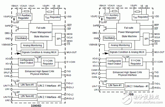
图1.MC33905内部框图
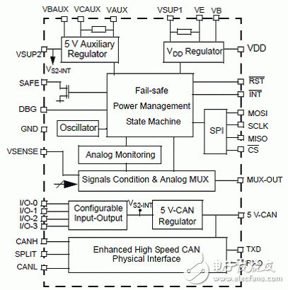
图2.MC33904内部框图
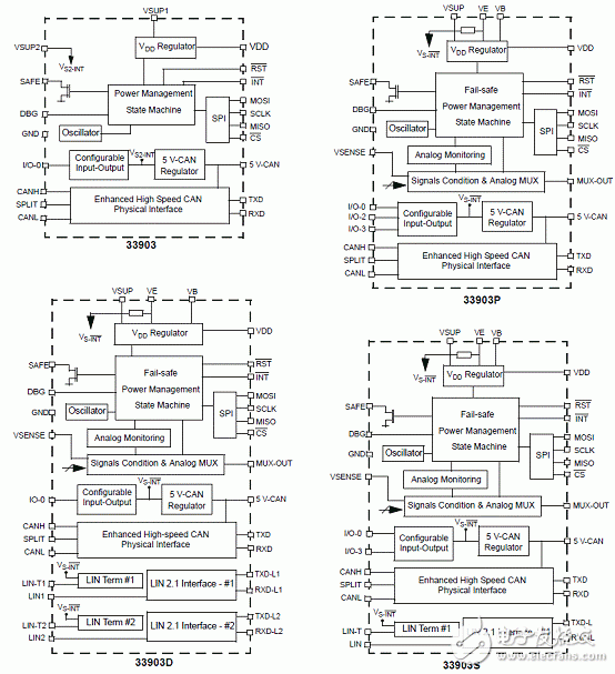
图3.MC33903内部框图
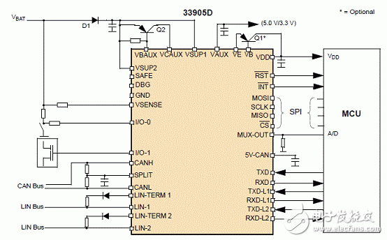
图4.MC33905D简化应用框图
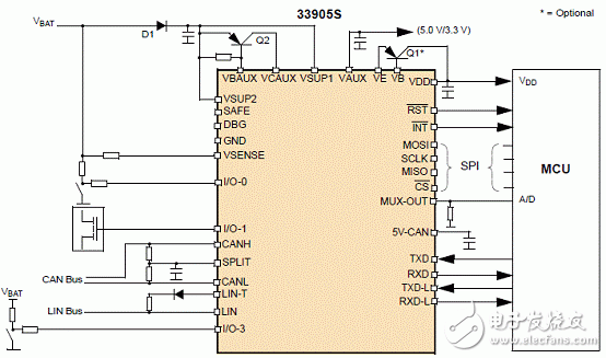
图5.MC33905S简化应用框图
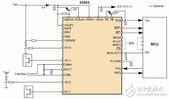
图6.MC33904简化应用框图
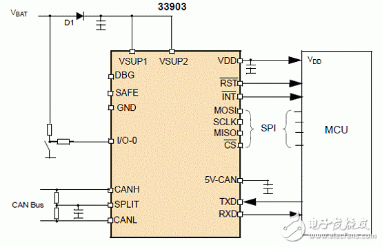
图7.MC33903简化应用框图
评估板KIT33905D5EKEVBE
The KIT33905D5EKEVBE supports the 33905D5 and 33904 devices, which are the second generation family of System Basis Chips, which combine several features and enhance present module designs. The devices work as an advanced power management unit for the MCU and additional integrated circuits such as sensors, CAN transceivers. They have a built-in enhanced high speed CAN interface (ISO11898-2 and -5), with local and bus failure diagnostics, protection, and fail safe operation mode. The SBCs may include one or two LIN 2.0 interfaces with LIN output pin switches. The 33904/5 include 2 or 3 wake-up input pins than can also be configured as output drivers for flexibility.
评估板KIT33905D5EKEVBE主要特性:
Nominal operating supply voltage range of 5.5 V to 27 V
Individually routed power supply inputs for VSUP1 and VSUP2
5.0/3.3 V regulator for MCU with an external PNP ballast transistor to increase current capability
Multiple CAN Bus termination options supported via socket
Two high/low side I/Os (SPI configurable) accessible through test points
Status of I/O-0 and I/O-1 indicated by an LED (dependent on jumper configuration)
Debug mode/watchdog configuration via jumper settings
MUX output voltage accessible through a test point and external resistor selectable through jumper
3.3 V or 5.0 V output voltage test point VAUX (SPI configurable)
I_WAKE_I test point to enable a FET and load VDD with current to wake-up the SBC
LIN1_T and LIN2_T test points to monitor I/O voltages (SPI configurable)
I/O-0, I/O-1, VAUX, 5V_CAN, SAFE, and VDD status indicated by LED
100 mil 2x8 pin standard header connector for SPI communication
100 mil 16 pin standard header connector for custom MCU board connections
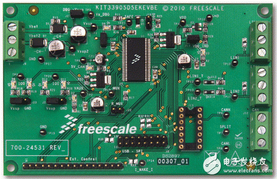
图8. 评估板KIT33905D5EKEVBE/KIT33905BD3EVBE外形图
评估板KIT33905D5EKEVBE/KIT33905BD3EVBE包括:
•KIT33905D5EKEVBE or KIT33905BD3EVBE Hardware
•CD33905 (includes SPIGen Software)
•CABLE, RIBBON FLAT 16 PIN ASSY, 0.100" PITCH, 6" LENGTH
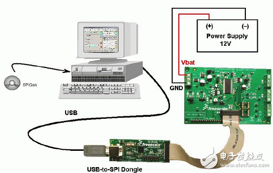
图9. 评估板KIT33905D5EKEVBE/KIT33905BD3EVBE建立配置图
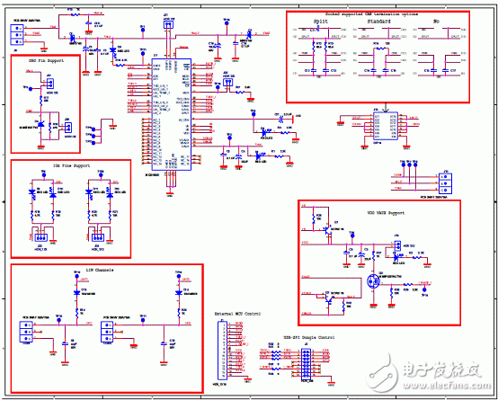
图10. 评估板KIT33905D5EKEVBE电路图
评估板KIT33905D5EKEVBE材料清单:
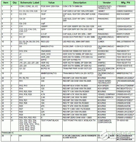
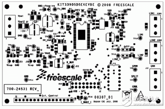
图11. 评估板KIT33905D5EKEVBE顶层PCB元件布局图
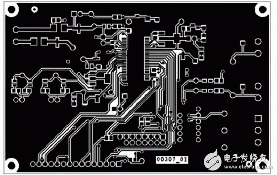
图12. 评估板KIT33905D5EKEVBE顶层PCB走线图
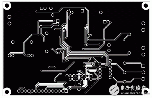
图13. 评估板KIT33905D5EKEVBE底层PCB走线图
-
bq5101x具有哪些特性参数应用?2021-05-25 0
-
AT86RF233具有哪些特性参数应用?2021-05-25 0
-
TDF8554J具有哪些特性参数应用?2021-06-01 0
-
PIC32 MCU具有哪些特性参数应用?2021-06-02 0
-
AK4678的主要特性是什么?其电路图是怎样的?2021-06-02 0
-
DRV8802-Q1主要特性 功能框图和应用电路2018-04-12 2108
-
FM0-64L-S6E1C3主要特性和,系统框图解析2018-04-28 2245
-
PIC32MZ嵌入连接MCU主要特性和框图分析2018-05-03 5872
-
MM912-S812小型摩托车引擎ECU参考设计(特性_系统框图_电路图_pcb元件布局)2018-06-07 8258
-
一文解析AK7736B主要特性_功能_电路图及PCB元件布局图2018-06-07 6734
-
AD8452主要特性_框图以及应用电路2019-05-11 7248
-
CC1352P主要特性以及pcb电路图2019-04-05 6813
-
NCP51705主要特性_内部框图以及应用电路2019-05-11 4002
-
Cypress PSoC®5开发板特性_电路图及PCB元件布局图2019-07-13 1290
全部0条评论

快来发表一下你的评论吧 !
