

ADI ADRF5020 30GHz RF开关解决方案
电子说
描述
ADI公司的ADRF5020是30GHz RF通用单刀双掷(SPDT)和单刀四掷(SP4T)开关,采用 20 引脚和 24 引脚基板栅格阵列(LGA)封装,提供高隔离度和高达30GHz的低插入损耗,超宽带频率范围为100 MHz至30 GHz,非反射式50 Ω设计,低插入损耗2.0 dB(30 GHz时),高隔离度60 dB(30 GHz时),高输入线性度,1 dB压缩(P1dB)28 dBm,三阶交调截点(IP3)52 dBm(典型值),主要用在测试测量,微波无线电和甚小孔径终端(VSAT)以及军用无线电,雷达,电子计数测量(ECM)和宽带通信系统。本文介绍了ADRF5020主要特性和功能框图,以及评估板ADRF5020-EVALZ主要特性,电路图,材料清单和PCB设计图。
The ADRF5020 is a general-purpose, single-pole, double-throw (SPDT) switch manufactured using a silicon process. It comes in a 3 mm × 3 mm, 20-terminal land grid array (LGA) package and provides high isolation and low insertion loss from 100 MHz to 30 GHz.
This broadband switch requires dual supply voltages, +3.3 V and −2.5 V, and provides CMOS/LVTTL logic-compatible control.
The ADRF5020 requires a positive supply voltage applied to the VDD pin and a negative supply voltage applied to the VSS pin. Bypassing capacitors are recommended on the supply lines to minimize RF coupling.
The ADRF5020 is internally matched to 50 Ω at the RF common port (RFC) and the RF throw ports (RF1 and RF2); therefore, no external matching components are required. All of the RF ports are dc-coupled to 0 V, and no dc blocking is required at the RF ports when the RF line potential is equal to 0 V. The design is bidirectional; the RF input signal can be applied to the RFC port while the RF throw port (RF1 or RF2) is output or vice versa.
The ADRF5020 incorporates a driver to perform logic functions internally and to provide the user with the advantage of a simplified control interface. The driver features two digital control input pins, CTRL and EN.
ADRF5020主要特性:
Ultrawideband frequency range: 100 MHz to 30 GHz
Nonreflective 50 Ω design
Low insertion loss: 2.0 dB to 30 GHz
High isolation: 60 dB to 30 GHz
High input linearity
1 dB power compression (P1dB): 28 dBm typical
Third-order intercept (IP3): 52 dBm typical
High power handling
24 dBm through path
24 dBm terminated path
ESD sensitivity: Class 1, 1 kV human body model (HBM)
20-terminal, 3 mm × 3 mm, land grid array package
No low frequency spurious
Radio frequency (RF) settling time (to 0.1 dB of final RF output): 15 ns
ADRF5020应用:
Test instrumentation
Microwave radios and very small aperture terminals (VSATs)
Military radios, radars, electronic counter measures (ECMs)
Broadband telecommunications systems
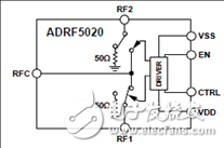
图1.ADRF5020功能框图
评估板ADRF5020-EVALZ
ADRF5020-EVALZ是一款配置齐全的4层RO4003评估板。正常工作时,需将两个电源电压+3.3 V和-2.5 V分别连接至DC测试点的VDD和VSS引脚,同时接地电压施加于DC测试点的GND引脚。
用于选择开关状态的两个0/+3.3 V控制电压施加于直流测试点的EN和CTRL。RF输入信号可施加于边缘安装型2.4mm RF连接器RFC,并在边缘安装型2.4mm RF连接器的RF1和RF2上测量RF输出信号。
All RF and dc traces are routed on the top copper layer whereas the inner and bottom layers are grounded planes that provide a solid ground for the RF transmission lines. Top dielectric material is 8 mil Rogers RO4003, offering good high frequency performance. The middle and bottom dielectric materials are FR-4 type materials to achieve an overall board thickness of 62 mil.
The RF transmission lines were designed using a coplanar waveguide (CPWG) model with a width of 14 mil and ground spacing of 5 mil to have a characteristic impedance of 50 Ω。 For good RF and thermal grounding, as many plated through vias as possible are arranged around transmission lines and under the exposed pad of the package.
Two control ports are connected to the EN and CTRL test points, TP3 and TP4. On each control trace, a resistor position is available to improve the isolation between the RF and control signals. The RF ports are connected to the RFC, RF1, and RF2 connectors (J1, J2, and J3) that are end launch 2.4 mm RF connectors. A through transmission line that connects unpopulated RF connectors (J7 and J8) is also available to measure the loss of the PCB. Figure 21 and Table 5 are the evaluation board schematic and bill of materials, respectively.
图2.评估板ADRF5020-EVALZ外形图
图3.评估板ADRF5020-EVALZ电路图
评估板ADRF5020-EVALZ材料清单:
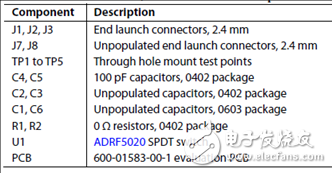
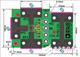
图4.评估板ADRF5020-EVALZ PCB布局图(顶视图)
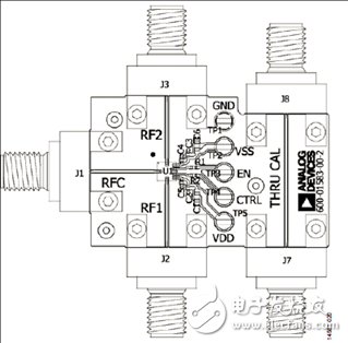
图5.评估板ADRF5020-EVALZ PCB元件分布图
-
ADRF5044BCCZN开关2018-07-04 0
-
预使用ADI两个开关产品,一组:ADRF5044/ADRF5045,二组:ADRF5020/ADRF5021,请问一组和二组开关可级联使用?2018-07-27 0
-
ADRF5044BCCZN开关ADI品牌2021-01-14 0
-
力科推出 4通道均为30GHz的实时示波器解决方案2010-02-08 863
-
力科推出4通道均为30GHz的实时示波器解决方案2010-02-11 1280
-
采用硅技术的开关取代PIN二极管2018-06-05 3634
-
ADRF5020 100 MHz至30 GHz硅SPDT开关2019-02-15 1166
-
ADRF5130/ADRF5020硅开关产品系列新产品2019-06-28 2537
-
ADRF5130和ADRF5020宽带硅开关的性能分析2019-06-14 2432
-
ADRF5020/ADRF5021 Gerber Files2021-02-21 441
-
ADRF5020 S-Parameters2021-03-10 398
-
ADRF5021:9 kHz至30 GHz、硅SPDT开关2021-03-21 482
-
ADRF5020:100 MHz对30 GHz,硅SPDT数据谢幕2021-04-30 410
-
ADRF50211 9 kHz至30 GHz,硅SPDT开关2021-06-01 432
-
ADRF5020 S参数2021-06-01 433
全部0条评论

快来发表一下你的评论吧 !
