

新一代智能电子化学传感器的新型传感器接口IC ADuCM355详解
电子说
描述
ADI公司的ADuCM355是新一代智能电子化学传感器的新型传感器接口IC,能够在单个芯片上同时实现恒电位仪和电化学阻抗频谱分析仪(EIS)功能的唯一解决方案。器件集成了行业最先进的传感器诊断技术,具有卓越的低噪声和低功耗性能,并且尺寸最小,显著节约成本。主要用在工业气体检测,仪器仪表,生命体征监测和疾病管理等。本文介绍了ADuCM355主要特性,功能框图,应用电路以及评估板EVAL-ADuCM355QSPZ主要特性和应用连接图。
The ADuCM355 is an on-chip system designed to control andmeasure electrochemical and biosensors. The ADuCM355 is an ultralow power mixed-signal microcontroller based on theARMRCortex™-M3 processor. It is designed with current, voltage, and impedance measurement capability. The ADuCM355 features a 16-bit, 400 kSPS multichannel successive approximation register (SAR) analog-to-digitalconverter (ADC) with input buffers, built in antialias filter(AAF) and programmable gain amplifier (PGA)。 The current inputs include three transimpedance amplifiers (TIA) with programmable gain and load resistors for measuring differentsensor types. The analog front end (AFE) also contains twomore low power amplifiers designed specifically for potentiostat capability to maintain a constant bias voltage to an external electrochemical sensor. The noninverting inputs of these twoamplifiers are controlled by on-chip dual output digital-to-analog converters (DAC)。 The analog outputs include anotherhigh speed DAC and output amplifier designed to generate an ac signal. The ADC is capable of operating at conversion rates up to 400 kSPS with an input range of ±0.9 V. An input mux before the ADC allows the user to select an input channel formeasurement. These input channels include three externalcurrent inputs, multiple external voltage inputs, and internal channels. The internal channels allow diagnostic measurementsof the internal supply voltages, die temperature, and referencevoltages. Two of the three voltage DACs are dual output, 12-bit stringDACs. One output per DAC controls the noninverting input of a potentiostat amplifier, and the other controls the noninverting input of the TIA.
The third DAC (sometimes referred to as the high speed DAC)is designed for the high power TIA for impedancemeasurements. Its output frequency range is up to 200 kHz. A precision 1.82 V and 2.5 V on-chip reference source is available. The internal ADC and VDAC circuits use this on-chip reference source to ensure low drift performance for all of these peripherals.
The ADuCM355 integrates a 26 MHz ARM Cortex-M3processor. It is a 32-bit reduced instruction set computer (RISC) machine, offering up to 32.5 DMIPS peak performance. The ARM Cortex-M3 processor also has a flexible multichannel direct memory access controller (DMA) supporting serial peripheral interface (two independent SPI ports), universalasynchronous receiver/transmitter (UART), and I2Ccommunication peripherals. The ADuCM355 has 128 kB of nonvolatile flash/EE memory and 64 kB of SRAM integrated on-chip. The digital processor subsystem is clocked from a 26 MHz on-chip oscillator. This is the source of the main digital die systemclock. Optionally, a 26 MHz PLL can be used as the digitalsystem clock. This clock can be internally subdivided so that the processor operates at a lower frequency and saves power. A lowpower internal 32 kHz oscillator is available and can clock thetimers. The ADuCM355 includes three general-purpose timers,a wake-up timer (which can be used as a general-purposetimer), and a system watchdog timer. The analog subsystem has a separate 16 MHz oscillator used to clock the ADC, DACs, and other digital logic on the analog die.
The analog die also contains a separate 32 kHz, low poweroscillator to clock a watchdog timer on the low voltage die. Both the 32 kHz oscillator and this watchdog are independent from the digital die oscillators and system watchdog timer. A range of communication peripherals can be configured asrequired in a specific application. These peripherals includeUART, I2C, 2xSPI, and GPIO ports. The GPIO, combined with the general-purpose timers, can be combined to generate apulse width modulation (PWM) type output. On-chip factory firmware supports in-circuit erasing of user flashtriggered via the UART, while nonintrusive emulation and programdownload are supported via the serial wire debug port (SW-DP) interface. The ADuCM355 operates from 2.8 V to 3.6 V supply and isspecified over a temperature range of −40℃ to +85℃。 The chip is packaged in a 72-lead 6 mm × 5 mm land grid array (LGA)package.
ADuCM355主要特性:
Analog input/output
16-bit, 400 kSPS ADC
Voltage, current, and impedance measurement capability
Internal/external current and voltage channels
Ultralow leakage switch matrix and input mux
Input buffers, programmable gain amplifier
Voltage DACs
2 dual output VDACs Output range 0.2 V to 2.4 V (±2.2 V voltage potential to sensor)
2 bias potentiostat and TIA amplifiers
Ultralow power, 1 μA per DAC
One high speed 12-bit VDAC
Output range to sensor ±607 mV
High speed TIA for impedance measurements
Programmable gain amplifier on output
Amplifiers, accelerators, and references 2 low power, low noise amplifiers
Suitable for potentiostat bias in electrochemical sensing
2 low power, low noise TIAs Suitable for measuring sensor current output 200 pA to 3 mA range Programmable load and gain resistors Analog hardware accelerators DDS waveform generator
DFT and digital filters 2.5 V and 1.82 V on-chip, precision voltage references Internal temperature sensor, ±2℃ accurate
Impedance measurement range of 《1 Ω to 10 MΩ, 1 Hz to 200 kHz
Voltammetry scan rate up to 2000 steps per second
Microcontroller
26 MHz ARM Cortex-M3 processor
Serial wire port supports code download and debug
128 kB flash/64 kB of SRAM
Security/safety
Hardware crypto accelerator with AES-128 and AES-256
Hardware CRC with programmable polynomial generator Read/write protection of user flash
On-chip peripherals
UART, I2C, and SPI serial input/output
Up to 10 GPIO pins
External interrupt option
General-purpose, wake-up, and watchdog timers
Power
2.8 V to 3.6 V supply and active measurement range
Power-supply monitor
Active current consumption 30 μA/MHz for digital part
Hibernate with bias to external sensor, 8.5 μA
Shutdown mode with no SRAM retention, 2 μA
Packages and temperature range
6 mm × 5 mm, 72-lead LGA package
Fully specified for −40℃ to +85℃ ambient operation
ADuCM355应用:
Gas detection Food quality
Environmental sensing (air, water, soil)
Blood glucose meters
Life sciences and biosensing analysis
Bioimpedance measurements
General Amperometry, voltammetry, and impedance
spectroscopy functions
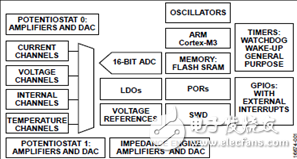
图1.ADuCM355简化功能框图
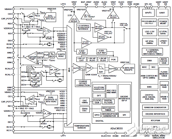
图2.ADuCM355功能框图
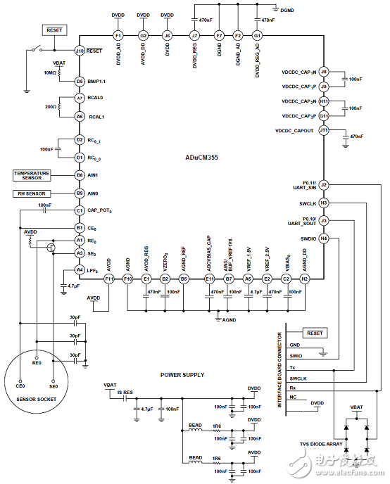
图3.ADuCM355推荐的外接元件连接图
评估板EVAL-ADuCM355QSPZ
The ADuCM355 system on a chip provides the features needed to bias and measure a range of different electrochemical sensors. The EVAL-ADuCM355QSPZ allows users to evaluate the performance of the ADuCM355 when implementing a range of different electrochemical techniques, including chronoam-perometry, voltammetry, and electrochemical impedance spectroscopy (EIS)。
评估板EVAL-ADuCM355QSPZ主要特性:
Debug/programming capability of ADuCM355
Evaluation capability with electrochemical gas sensors
ADT7420 0.5 C accurate temperature sensor via I2C
USB power option and connection to PC
图4.评估板EVAL-ADuCM355QSPZ外形图
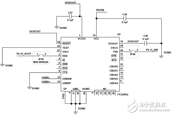
图5.JP45和JP46连接ADuCM355 UART引脚到USB收发器
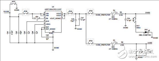
图6.LDO和电源周围跳线部分电路图
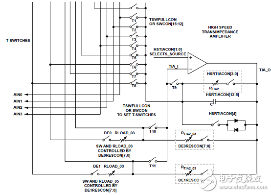
图7.HSTIA可编增益电阻
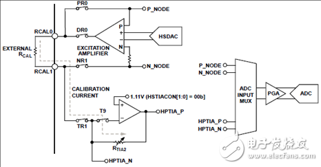
图8.用来RTIA2校准的HSDAC HSTIA和开关矩阵设定图
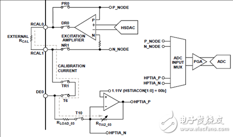
图9.用于RTIA2_03校准的HSDAC HSTIA和开关矩阵设定图
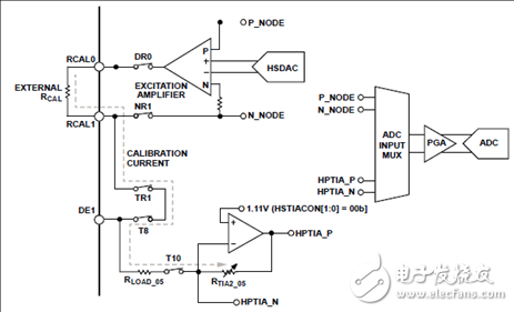
图10.用于RTIA2_05校准的HSDAC HSTIA和开关矩阵设定图
-
aducm355内部的温度传感器怎么使用?p2.1口的中断是怎么产生的?2024-01-11 0
-
ADUCM355 ADC是否可以设为差动输入模式?2024-01-11 0
-
开发新型传感器的途径2017-09-25 0
-
浅析化学传感器和纳米传感器2019-07-02 0
-
基于微型传感器的汽车电子化智能化工程应用2019-07-26 0
-
汽车中的传感器原理是什么2020-05-20 0
-
分析仪和传感器等以智能化为主2020-05-20 0
-
新一代磁性位置传感器助力无人机、轻工业、医疗以及太空机器人应用有哪些?2020-08-10 0
-
ADI推出新型传感器接口IC2018-06-29 592
-
ADI推出新型智能电子化学传感器接口IC—ADuCM3552018-06-28 10468
-
ADI推出新一代智能电子化学传感器的新型传感器接口 IC重磅来袭2018-07-04 3459
-
ADUCM355 具有化学传感器接口的精密模拟微控制器2019-02-22 941
-
ADuCM355和LTC6078解决方案2019-06-28 1930
-
ADuCM355如何提升电化学气体传感器的性能2019-06-28 3575
全部0条评论

快来发表一下你的评论吧 !
