

[原创] Infineon Xilinx Ultra Scale KintexFPGA开发方案
嵌入式技术
描述
KintexUltraScale套件基于Xilinx公司的KintexUltraScale XCKU040-1FBVA676 FPGA器件,包涵了开发嵌入式处理系统所有需要的功能.本文介绍了KintexUltraScale开发板主要特性,框图,开发板接口位置图和电路图.
The Xilinx Kintex® UltraScale™ Development Kit provides a complete development platform for designing and verifying applications based on the Xilinx KintexUltraScale All Programmable FPGA devices. The Xilinx KintexUltraScale development board packages all the necessary functions needed for an embedded processing system.
Available with the KintexUltraScale XCKU040-1FBVA676 device, the KintexUltraScale kit enables designers to prototype high-performance designs with ease, while providing expandability and customization through the FMC HPC expansion slot and PMOD headers. In addition to the Xilinx KintexUltraScale XCKU040 device, the KintexUltraScale development board features 1GB DDR4 SDRAM, two SFP+ interfaces, dual QSPI Flash memories, HDMI interface, LVDS touch panel interface, two 10/100/1000 Ethernet PHYs, and a USB-UART port.
KintexUltraScale开发板主要特性:
Xilinx XCKU040-1FBVA676 FPGA
1GB DDR4 SDRAM (x32 @ 1600Mbps)
32MB of Configuration QSPI Flash (single QSPI x4)
32MB of User Code/Data QSPI Flash (single QSPI x4)
Two 10/100/1000 Ethernet Interfaces (RGMII)
USB-UART Interface
FMC HPC Slot (VADJ of 1.8V, 2.5V, or 3.3V)
Two SFP+ Interfaces (up to 12.5Gbps)
Two GTH SMA Interfaces (up to 12.5Gbps)
LVDS Touch Panel Interface
Four PMOD headers
HDMI Interface
8 User LEDs
5 User Push Switches
8 User DIP Switches
Programmable LVDS Clock Source (GTH reference clock)
250 MHz LVDS Oscillator (system clock)
JTAG Header
SYSMON Header
Digilent USB-JTAG Module (JTAG-SMT2)
KintexUltraScale开发板目标应用:
Embedded controllers
General-purpose prototyping
Networking and communications
Storage and servers
Video applications
KintexUltraScale开发板包括:
硬件:
Avnet KintexUltraScale Development Board XCKU040-1FBVA676 KintexUltraScale FPGA device
Ethernet and USB A-mini-B Cables (2)
12V Power Supply (US/UK/ Euro AC cords)
软件工具:
Xilinx Vivado: Design Edition (Device locked to XCKU040
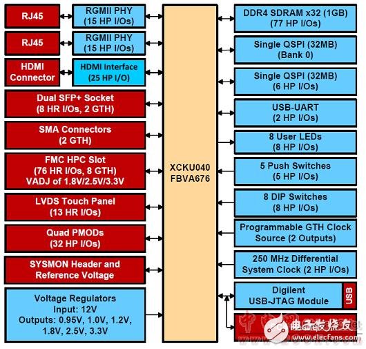
图1.KintexUltraScale开发板框图
图2.KintexUltraScale开发板接口位置图
图3.KintexUltraScale开发板PCB尺寸图
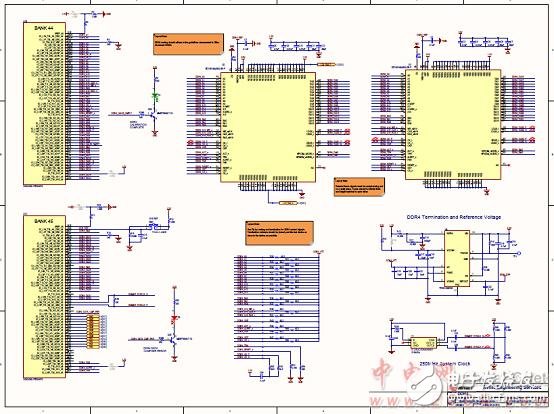
图4.KintexUltraScale开发板电路图(1)
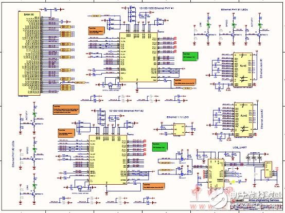
图5.KintexUltraScale开发板电路图(2)
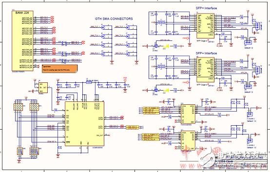
图6.KintexUltraScale开发板电路图(3)
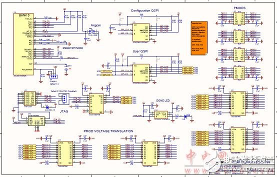
图7.KintexUltraScale开发板电路图(4)
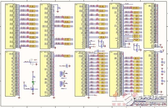
图8.KintexUltraScale开发板电路图(5)
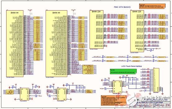
图9.KintexUltraScale开发板电路图(6)
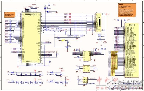
图10.KintexUltraScale开发板电路图(7)
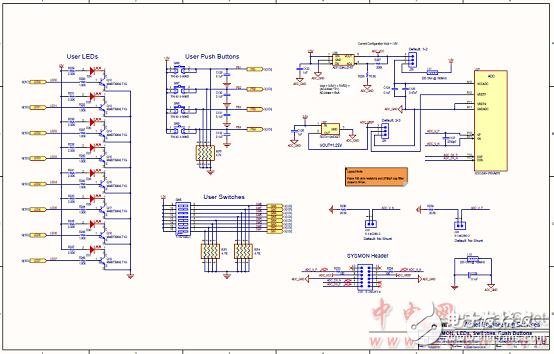
图11.KintexUltraScale开发板电路图(8)
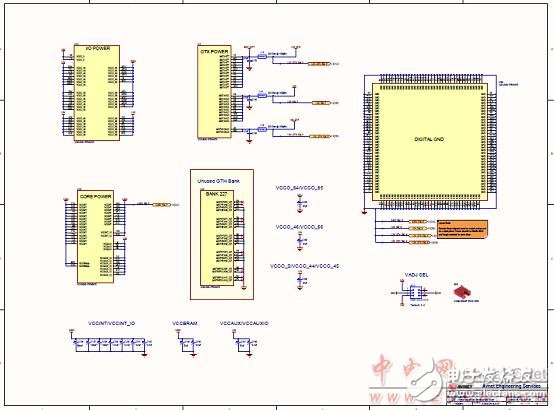
图12.KintexUltraScale开发板电路图(9)
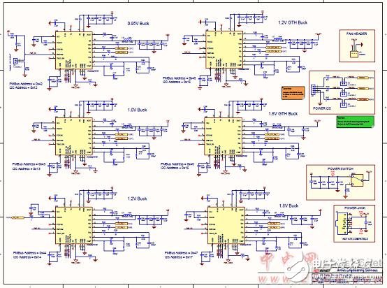
图13.KintexUltraScale开发板电路图(10)
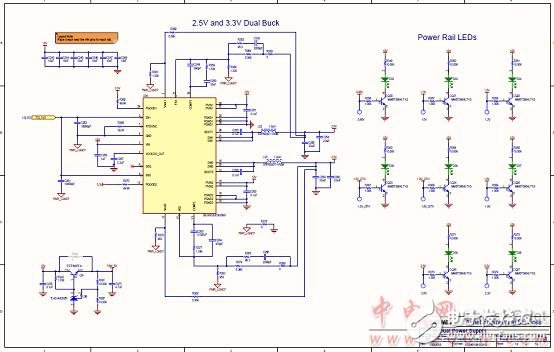
图14.KintexUltraScale开发板电路图(11)
图15.KintexUltraScale开发板电路图(12)
详情请见:
infineon.com/dgdl/Infineon-kit_kintexultrascale_pb_v3a-PB-v01_00-EN.pdf?fileId=5546d462525dbac40152f8c2a36d6a32">?fileId=5546d462525dbac40152f8c2a36d6a32
和?fileId=5546d462525dbac40152f8d4d74b6a51
以及?fileId=5546d462525dbac40152f8b98bc56a24
Infineon-AES_KU040_DB_G_User_Guide-UM-v01_00-EN.pdf
Infineon-kit_Kintex_Ultrascale_devkit_Schematics-ATI-v01_00-EN.pdf
Infineon-kit_kintexultrascale_pb_v3a-PB-v01_00-EN.pdf
Infineon-BOM_AES_KU040_DB_G-ATI-v01_00-EN.xls
- 相关推荐
-
#硬声创作季 #FPGA Xilinx入门-16 亚稳态现象原理与解决方案-1水管工 2022-10-09
-
#硬声创作季 #FPGA Xilinx入门-16 亚稳态现象原理与解决方案-2水管工 2022-10-09
-
#硬声创作季 #FPGA Xilinx入门-16 亚稳态现象原理与解决方案-3水管工 2022-10-09
-
#硬声创作季 #FPGA Xilinx入门-16 亚稳态现象原理与解决方案-4水管工 2022-10-09
-
#硬声创作季 #FPGA Xilinx入门-16 亚稳态现象原理与解决方案-5水管工 2022-10-09
-
Xilinx FPGA EDK开发实例2012-08-15 0
-
Xilinx FPGA开发实用教程(第2版)-徐文波、田耘2012-07-31 11380
-
Xilinx_FPGA系列入门教程(一)—如何搭建Xilinx2016-01-18 698
-
Large-Scale_FPGA-based_Convolutional_Networks2016-03-24 528
-
Xilinx-FPGA高级开发工具2016-09-01 823
-
基于Xilinx FPGA的开发板及代码2017-09-01 797
-
Xilinx FPGA电源TI解决方案(1)2018-08-22 3217
-
Xilinx FPGA电源TI解决方案(2)2018-08-21 2271
-
Xilinx FPGA开发实用教程2022-04-18 587
全部0条评论

快来发表一下你的评论吧 !
