

DRV835x用于三相马达的三相智能栅极驱动器
电子说
描述
TI公司的DRV835x系列是用于三相马达的9-100V三相智能栅极驱动器,集成了用于高边和低边的三个独立半桥栅极驱动器,电荷泵和线性稳压器,以及可选择的三个电流分流放大器和350mA降压稳压器,工作电压6-95V,输出电流2.5V-75V/350mA.主要用在3相无刷DC(BLDC)马达模块,风扇,鼓风机和泵,电动自行车,电动滑板车和电动汽车,无人机,机器人遥控玩具,工厂自动化和纺织机械。本文介绍了DRV835x系列主要特性和框图,栅极驱动器框图,应用电路以及评估板DRV8353RS-EVM主要特性和电路图,材料清单与PCB设计图。
The DRV835x family of devices are integrated 100-V gate drivers for three-phase motor drive applications.
These devices decrease system component count, cost, and complexity by integrating three independent halfbridgegate drivers, charge pump and linear regulator for the high-side and low-side gate driver supply voltages,optional triple current shunt amplifiers, and an optional 350-mA buck regulator. A standard serial peripheralinterface (SPI) provides a simple method for configuring the various device settings and reading fault diagnosticinformation through an external controller. Alternatively, a hardware interface (H/W) option allows for configuringthe most commonly used settings through fixed external resistors.
The gate drivers support external N-channel high-side and low-side power MOSFETs and can drive up to 1-Asource, 2-A sink peak currents with a 25-mA average output current. The high-side gate drive supply voltage isgenerated using a doubler charge-pump architecture that regulates the VCP output to VVDRAIN + 10.5-V. The lowsidegate drive supply voltage is generated using a linear regulator from the VM power supply that regulates theVGLS output to 14.5-V. The VGLS supply is further regulated to 11-V on the GLx low-side gate driver outputs. Asmart gate-drive architecture provides the ability to dynamically adjust the output gate-drive current strengthallowing for the gate driver to control the power MOSFET VDS switching speed. This allows for the removal ofexternal gate drive resistors and diodes reducing BOM component count, cost, and PCB area. The architecturealso uses an internal state machine to protect against gate-drive short-circuit events, control the half-bridge deadtime, and protect against dV/dt parasitic turnon of the external power MOSFET.
The gate drivers can operate in either a single or dual supply architecture. In the single supply architecture, VMcan be tied to VDRAIN and is regulated to the correct supply voltages internally. In the dual supply architecture,VM can be connected to a lower voltage supply from a more efficient switching regulator to improve the deviceefficiency. VDRAIN stays connected to the external MOSFETs to set the correct charge pump and overcurrentmonitor reference.
The DRV8353 and DRV8353R devices integrate three, bidirectional current-shunt amplifiers for monitoring thecurrent level through each of the external half-bridges using a low-side shunt resistor. The gain setting of theshunt amplifier can be adjusted through the SPI or hardware interface with the SPI providing additional flexibilityto adjust the output bias point.
The DRV8350R and DRV8353R devices integrate a 350-mA buck regulator that can be used to power anexternal controller or other logic circuits. The buck regulator is implemented as a separate internal die that canuse either the same or a different power supply from the gate driver.
In addition to the high level of device integration, the DRV835x family of devices provides a wide range ofintegrated protection features. These features include power-supply undervoltage lockout (UVLO), gate driveundervoltage lockout (GDUV), VDS overcurrent monitoring (OCP), gate-driver short-circuit detection (GDF), andovertemperature shutdown (OTW/OTSD)。 Fault events are indicated by the nFAULT pin with detailed informationavailable in the SPI registers on the SPI device version.
The DRV835x family of devices are available in 0.5-mm pin pitch, QFN surface-mount packages. The QFN sizesare 5 × 5 mm for the 32-pin package, 6 × 6 mm for the 40-pin package, and 7 × 7 mm for the 48-pin package.
DRV8353RS主要特性:
1• 9 to 100-V, Triple Half-Bridge Gate Driver
– Optional Integrated Buck Regulator
– Optional Triple Low-Side Current ShuntAmplifiers
• Smart Gate Drive Architecture
– Adjustable Slew Rate Control For EMIPerformance
– VGS Handshake and Minimum Dead-TimeInsertion to Prevent Shoot-Through
– 50-mA to 1-A Peak Source Current
– 100-mA to 2-A Peak Sink Current
– dV/dt Mitigation Through Strong Pulldown
• Integrated Gate Driver Power Supplies
– High-Side Doubler Charge Pump For 100%PWM Duty Cycle Control
– Low-Side Linear Regulator
• Integrated LM5008A Buck Regulator
– 6 to 95-V Operating Voltage Range
– 2.5 to 75-V, 350-mA Output Capability
• Integrated Triple Current Shunt Amplifiers
– Adjustable Gain (5, 10, 20, 40 V/V)
– Bidirectional or Unidirectional Support
• 6x, 3x, 1x, and Independent PWM Modes
– Supports 120° Sensored Operation
• SPI or Hardware Interface Available
• Low-Power Sleep Mode (20 μA at VVM = 48-V)
• Integrated Protection Features
– VM Undervoltage Lockout (UVLO)
– Gate Drive Supply Undervoltage (GDUV)
– MOSFET VDS Overcurrent Protection (OCP)
– MOSFET Shoot-Through Prevention
– Gate Driver Fault (GDF)
– Thermal Warning and Shutdown (OTW/OTSD)
– Fault Condition Indicator (nFAULT)
DRV8353RS应用:
• 3-Phase Brushless-DC (BLDC) Motor Modules
• Fans, Blowers, and Pumps
• E-Bikes, E-Scooters, and E-Mobility
• Power and Garden Tools, Lawn Mowers
• Drones, Robotics, and RC Toys
• Factory Automation and Textile Machines
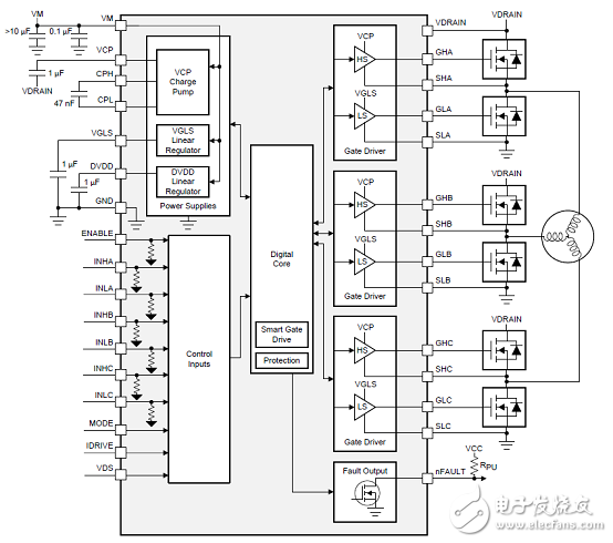
图1.DRV8350H框图
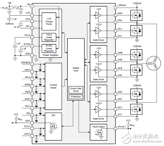
图2.DRV8350S框图
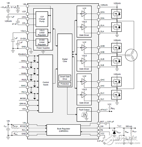
图3.DRV8350RH框图
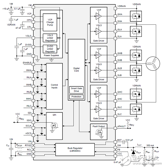
图4.DRV8350RS框图
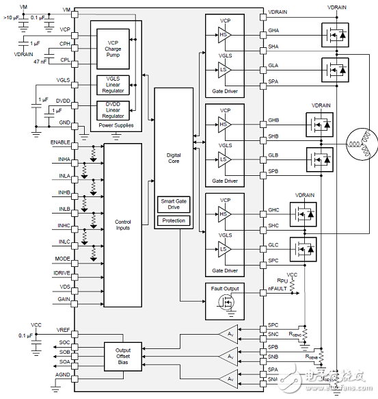
图5.DRV8353H框图
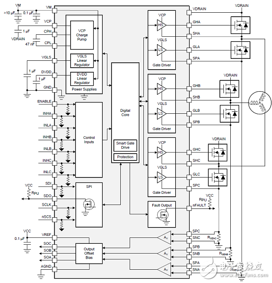
图6.DRV8353S框图
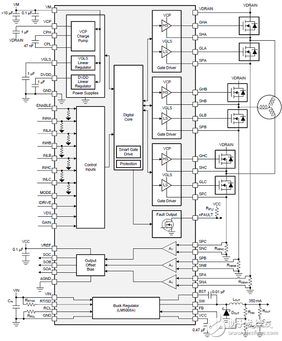
图7.DRV8353RH框图
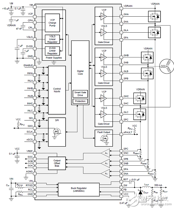
图8.DRV8353RS框图
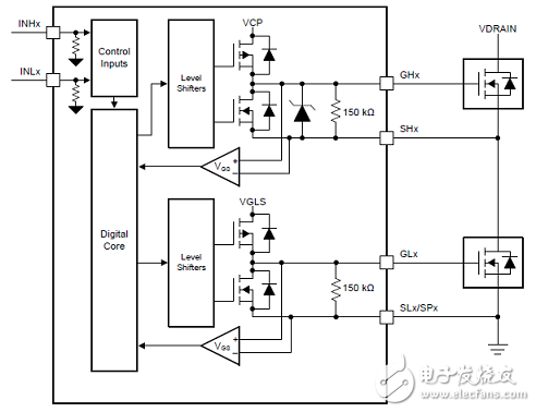
图9.栅极驱动器框图
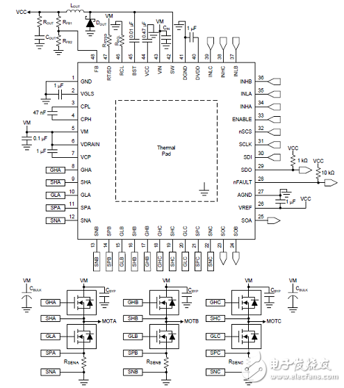
图10.DRV8353系列基本应用电路图(1)
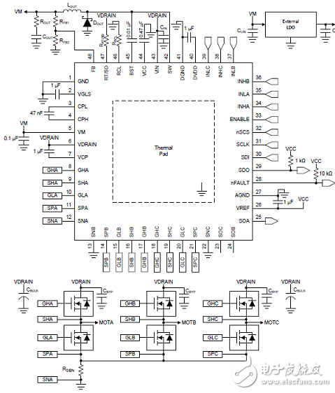
图11.DRV8353系列基本应用电路图(2)
评估板DRV8353RS-EVM
The DRV8353RS-EVM is a 15A, 3-phase brushless DC drive stage based on the DRV8353RS gate driver and CSD19532Q5B NexFET™ MOSFETs.
The module has individual DC bus and phase voltage sense as well as individual low-side current shunt amplifiers, making this evaluation module ideal for sensorless BLDC algorithms. The module supplies MCU 3.3V power with an integrated 0.35A step down buck regulator. The drive stage has IDRIVE configuration, along with a fault pin and protection for short circuit, thermal, shoot-through, and under voltage conditions through configurable SPI.
评估板DRV8353RS-EVM主要特性:
9- to 95-V operation
15 A continuous/20 A peak H-bridge output current
Internal buck regulator
Three individual, internal low-side current shunt amplifiers
INSTASPIN FOC BLDC firmware available
图12.评估板DRV8353RS-EVM外形图
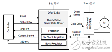
图13.评估板DRV8353RS-EVM框图
图14.评估板DRV8353RS-EVM硬件连接图(1)
图15.评估板DRV8353RS-EVM硬件连接图(2)
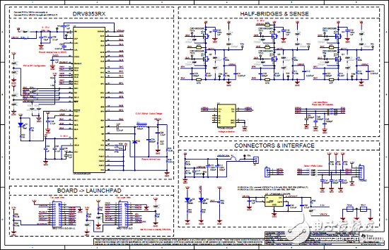
图16.评估板DRV8353Rx-EVM电路图(1):MD016A
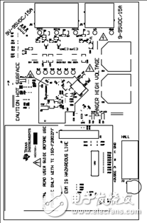
图17.评估板DRV8353Rx-EVM MD016A PCB设计图(1)
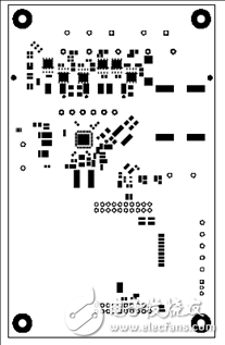
图18.评估板DRV8353Rx-EVM MD016A PCB设计图(2)
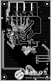
图19.评估板DRV8353Rx-EVM MD016A PCB设计图(3)
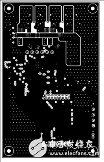
图20.评估板DRV8353Rx-EVM MD016A PCB设计图(4)
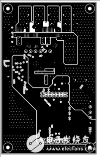
图21.评估板DRV8353Rx-EVM MD016A PCB设计图(5)
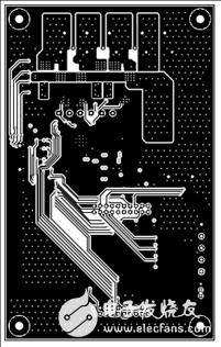
图22.评估板DRV8353Rx-EVM MD016A PCB设计图(6)
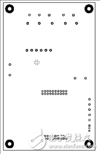
图23.评估板DRV8353Rx-EVM MD016A PCB设计图(7)
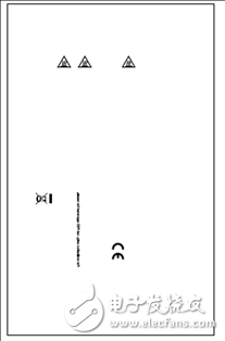
图24.评估板DRV8353Rx-EVM MD016A PCB设计图(8)
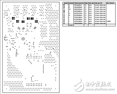
图25.评估板DRV8353Rx-EVM MD016A PCB设计图(9)
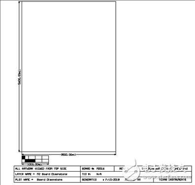
图26.评估板DRV8353Rx-EVM MD016A PCB设计图(10)
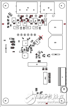
图27.评估板DRV8353Rx-EVM MD016A(001)装配图
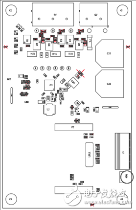
图28.评估板DRV8353Rx-EVM MD016A(002)装配图
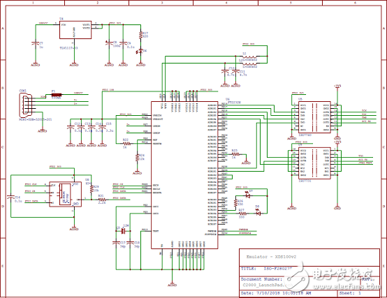
图29.评估板DRV8353Rx-EVM MD017A电路图(1)
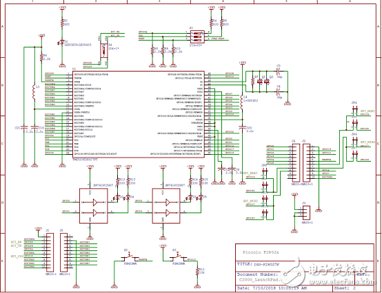
图30.评估板DRV8353Rx-EVM MD017A电路图(2)
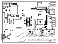
图31.评估板DRV8353Rx-EVM MD017A PCB设计图(1)
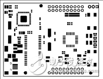
图32.评估板DRV8353Rx-EVM MD017A PCB设计图(2)
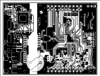
图33.评估板DRV8353Rx-EVM MD017A PCB设计图(3)
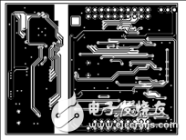
图34.评估板DRV8353Rx-EVM MD017A PCB设计图(4)
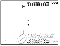
图35.评估板DRV8353Rx-EVM MD017A PCB设计图(5)
图36.评估板DRV8353Rx-EVM MD017A PCB设计图(6)
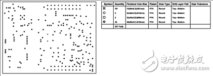
图37.评估板DRV8353Rx-EVM MD017A PCB设计图(7)

图38.评估板DRV8353Rx-EVM MD017A PCB设计图(8)
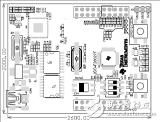
图39.评估板DRV8353Rx-EVM MD017A PCB装配图(1)
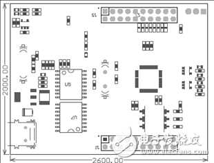
图39.评估板DRV8353Rx-EVM MD017A PCB装配图(2)
评估板DRV8353Rx-EVM材料清单见:
MCU036A(001)_BOM.xls
MD016A(001)_BOM.xls
MD016A(002)_BOM.xls
slvc742a.zip
详情请见:
和
drv8353.pdf
-
用于三相逆变器的宽输入隔离型 IGBT 栅极驱动 Fly-Buck 电源2015-03-23 0
-
600V三相栅极驱动器IC2016-06-21 0
-
IRS26302D:保护式600V三相栅极驱动器2016-06-21 0
-
用于三相逆变器的IGBT栅极驱动隔离型电源包括BOM及层图2018-09-06 0
-
工业驱动器的三相紧凑型功率级参考设计包括BOM及框图2018-09-30 0
-
三相BLDC/PMSM电机控制评估套件2018-11-12 0
-
三相逆变器的隔离式IGBT栅极驱动器评估系统设计2018-12-27 0
-
用于三相电机驱动的L6386 MOSFET功率驱动器评估板AN13152019-07-03 0
-
用于驱动三相或两相电机的一种交流/直流逆变器2020-05-29 0
-
简化48V至60V直流馈电三相逆变器设计的方法2020-10-27 0
-
基于DRV8353RH的三相智能栅极驱动器评估模块电路该如何去设计?2021-07-02 0
-
如何对三相无刷电机驱动器进行仿真?2021-07-21 0
-
三相无刷马达驱动电路2021-07-24 0
-
基于DRV8301的三相无刷直流电机驱动器参考设计2022-09-28 0
-
三相马达驱动用的栅极驱动器DRV8305-Q1的主要特性2018-04-27 9066
全部0条评论

快来发表一下你的评论吧 !
