

详解Xilinx公司Zynq® UltraScale+™MPSoC产品
汽车电子
描述
Avnet公司的Ultra96 开发板是基于ARM的Xilinx ZynqUltraScale+™ MPSoC系列产品的满足Linaro 96板指标的开发板,设计者可创建或评估Zynq处理器子系统(PS)和可编逻辑(PL)架构,主要用在航空航天与国防,汽车电子,数据中心,无线通信基础设备和无线基础设施.本文介绍了Xilinx公司的Zynq® UltraScale+™MPSoC系列主要特性,应用方案以及AvnetUltra96开发板主要特性,框图,电路图,材料清单和PCB设计图.
Zynq® UltraScale+™ All Programmable MPSoCs provide up to 5X systemlevelperformance-per-watt compared to the Zynq-7000 SoC family.
ZynqUltraScale+ devices combine a high-performance ARM®-basedmulticore,multiprocessing system with ASIC-class programmable logic.
Dual- and quad-core application processor equipped devices delivermaximum scalability, and are capable of offloading critical applications,such as graphics and video pipelining, to dedicated processing blocks,along with a full complement of integrated peripherals and connectivitycores suitable for next-generation systems.
For the most compute intensive processing tasks, integratedprogrammable logic offers up to 100X performance improvement overprocessor-based implementations. The 16nm FinFET+ programmablelogic communicates with the processing system through 6,000 interconnects, enabling bandwidth that is not possible with multichipsolutions. Dramatic power savings are achieved through fine-grainedcontrol of power domains and gated power islands. With specializedprocessing elements for different workloads, ZynqUltraScale+ MPSoCsintegrate the right engines for the right tasks for next-generation
embedded challenges.
Ultra96™ is an Arm-based, Xilinx ZynqUltraScale+™ MPSoC development board based on the Linaro 96Boards specification.
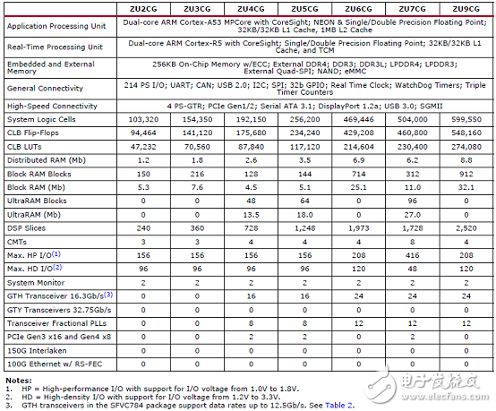
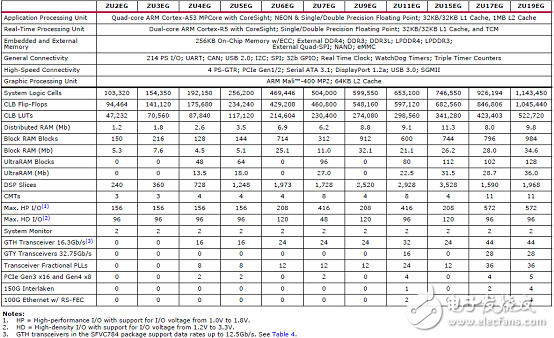
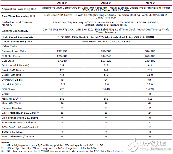
The Zynq® UltraScale+™ MPSoC family is based on the Xilinx® UltraScale™ MPSoC architecture. Thisfamily of products integrates a feature-rich 64-bit quad-core or dual-core ARM® Cortex™-A53 anddual-core ARM Cortex-R5 based processing system (PS) and Xilinx programmable logic (PL)UltraScalearchitecture in a single device. Also included are on-chip memory, multiport external memory interfaces,and a rich set of peripheral connectivity interfaces.
Zynq® UltraScale+™ MPSoC系列主要特性:
Processing System (PS)
ARM Cortex-A53 Based ApplicationProcessing Unit (APU)
• Quad-core or dual-core
• CPU frequency: Up to 1.5GHz
• Extendable cache coherency
• ARMv8-A Architecture
o 64-bit or 32-bit operating modes
oTrustZone security
o A64 instruction set in 64-bit mode,A32/T32 instruction set in 32-bit mode
• NEON Advanced SIMD media-processing engine
• Single/double precision Floating Point Unit (FPU)
• CoreSight™ and Embedded Trace Macrocell (ETM)
• Accelerator Coherency Port (ACP)
• AXI Coherency Extension (ACE)
• Power island gating for each processor core
• Timer and Interrupts
o ARM Generic timers support
o Two system level triple-timer counters
o One watchdog timer
o One global system timer
• Caches
o 32KB Level 1, 2-way set-associativeinstruction cache with parity (independent for
each CPU)
o 32KB Level 1, 4-way set-associative datacache with ECC (independent for each CPU)
o 1MB 16-way set-associative Level 2 cachewith ECC (shared between the CPUs)
Dual-core ARM Cortex-R5 BasedReal-Time Processing Unit (RPU)
• CPU frequency: Up to 600MHz
• ARMv7-R Architecture
o A32/T32 instruction set
• Single/double precision Floating Point Unit (FPU)
• CoreSight™ and Embedded Trace Macrocell(ETM)
• Lock-step or independent operation
• Timer and Interrupts:
o One watchdog timer
o Two triple-timer counters
• Caches and Tightly Coupled Memories (TCMs)
o 32KB Level 1, 4-way set-associativeinstruction and data cache with ECC
(independent for each CPU)
o 128KB TCM with ECC (independent for eachCPU) that can be combined to become 256KBin lockstep mode
On-Chip Memory
• 256KB on-chip RAM (OCM) in PS with ECC
• Up to 36Mb on-chip RAM (UltraRAM) with ECC inPL
• Up to 35Mb on-chip RAM (block RAM) with ECCin PL
• Up to 11Mb on-chip RAM (distributed RAM) in PL
ARM Mali-400 Based GPU
• Supports OpenGL ES 1.1 and 2.0
• Supports OpenVG 1.1
• GPU frequency: Up to 667MHz
• Single Geometry Processor, Two Pixel Processors
• Pixel Fill Rate: 2 Mpixels/sec/MHz
• Triangle Rate: 0.11 Mtriangles/sec/MHz
• 64KB L2 Cache
• Power island gating
External Memory Interfaces
• Multi-protocol dynamic memory controller
• 32-bit or 64-bit interfaces to DDR4, DDR3,DDR3L, or LPDDR3 memories, and 32-bit
interface to LPDDR4 memory
• ECC support in 64-bit and 32-bit modes
• Up to 32GB of address space using single or dualrank of 8-, 16-, or 32-bit-wide memories
• Static memory interfaces
o eMMC4.51 Managed NAND flash support
o ONFI3.1 NAND flash with 24-bit ECC
o 1-bit SPI, 2-bit SPI, 4-bit SPI (Quad-SPI), ortwo Quad-SPI (8-bit) serial NOR flash
8-Channel DMA Controller
• Two DMA controllers of 8-channels each
• Memory-to-memory, memory-to-peripheral,peripheral-to-memory, and scatter-gather transaction support
Serial Transceivers
• Four dedicated PS-GTR receivers andtransmitters supports up to 6.0Gb/s data rates
o Supports SGMII tri-speed Ethernet, PCIExpress® Gen2, Serial-ATA (SATA), USB3.0,and DisplayPort Dedicated I/O Peripherals andInterfaces
• PCI Express — Compliant with PCIe® 2.1 basespecification
o Root complex and End Point configurations
o x1, x2, and x4 at Gen1 or Gen2 rates
• SATA Host
o 1.5, 3.0, and 6.0Gb/s data rates as defined bySATA Specification, revision 3.1
o Supports up to two channels
• DisplayPort Controller
o Up to 5.4Gb/s rate
o Up to two TX lanes (no RX support)
• Four 10/100/1000 tri-speed Ethernet MACperipherals with IEEE Std 802.3 and IEEE Std 1588revision 2.0 support
o Scatter-gather DMA capability
o Recognition of IEEE Std 1588 rev.2 PTP frames
o GMII, RGMII, and SGMII interfaces
o Jumbo frames
• Two USB 3.0/2.0 Device, Host, or OTG peripherals,each supporting up to 12 endpoints
o USB 3.0/2.0 compliant device IP core
o Super-speed, high- speed, full-speed, andlow-speed modes
o Intel XHCI- compliant USB host
• Two full CAN 2.0B-compliant CAN bus interfaces
o CAN 2.0-A and CAN 2.0-B and ISO 118981-1standard compliant
• Two SD/SDIO 2.0/eMMC4.51 compliantcontrollers
• Two full-duplex SPI ports with three peripheralchip selects
• Two high-speed UARTs (up to 1Mb/s)
• Two master and slave I2C interfaces
• Up to 78 flexible multiplexed I/O (MIO) (up tothree banks of 26 I/Os) for peripheral pin
assignment
• Up to 96 EMIOs (up to three banks of 32 I/Os)connected to the PL
Interconnect
• High-bandwidth connectivity within PSand between PS and PL
• ARM AMBA® AXI4-based
• QoS support for latency and bandwidth control
• Cache Coherent Interconnect (CCI)
System Memory Management
• System Memory Management Unit (SMMU)
• Xilinx Memory Protection Unit (XMPU)
Platform Management Unit
• Power gates PS peripherals, power islands, andpower domains
• Clock gates PS peripheral user firmware option
Configuration and Security Unit
• Boots PS and configures PL
• Supports secure and non-secure boot modes
System Monitor in PS
• On-chip voltage and temperature sensing
Programmable Logic (PL)
Configurable Logic Blocks (CLB)
• Look-up tables (LUT)
• Flip-flops
• Cascadable adders
36Kb Block RAM
• True dual-port
• Up to 72 bits wide
• Configurable as dual 18Kb
UltraRAM
• 288Kb dual-port
• 72 bits wide
• Error checking and correction
DSP Blocks
• 27 x 18 signed multiply
• 48-bit adder/accumulator
• 27-bit pre-adder
Programmable I/O Blocks
• Supports LVCMOS, LVDS, and SSTL
• 1.0V to 3.3V I/O
• Programmable I/O delay and SerDes
JTAG Boundary-Scan
• IEEE Std 1149.1 Compatible Test Interface
PCI Express
• Supports Root complex and End Pointconfigurations
• Supports up to Gen4 speeds
• Up to five integrated blocks in select devices
100G Ethernet MAC/PCS
• IEEE Std 802.3 compliant
• CAUI-10 (10x 10.3125Gb/s) or
CAUI-4 (4x 25.78125Gb/s)
• RSFEC (IEEE Std 802.3bj) in CAUI-4 configuration
• Up to four integrated blocks in select devices
Interlaken
• Interlaken spec 1.2 compliant
• 64/67 encoding
• 12 x 12.5Gb/s or 6 x 25Gb/s
• Up to four integrated blocks in select devices
Video Encoder/Decoder (VCU)
• Available in EV devices
• Accessible from either PS or PL
• Simultaneous encode and decode
• H.264 and H.265 support
System Monitor in PL
• On-chip voltage and temperature sensing
• 10-bit 200KSPS ADC with up to 17 external inputs
ZynqUltraScale+ MPSoC: CG器件主要特性:
ZynqUltraScale+ MPSoC: EG器件主要特性:
ZynqUltraScale+ MPSoC: EV器件主要特性:
ZynqUltraScale+ MPSoC系列目标应用:
• Aerospace & Defense
• Automotive
• Data Center
• Wired Communications Infrastructure
• Wireless Infrastructure
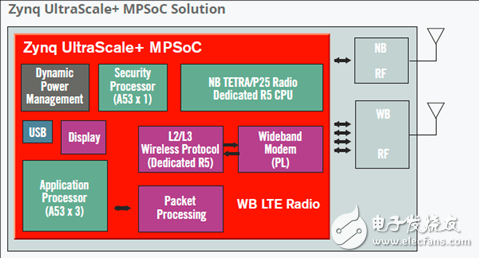
应用案例1:
基于照相机的高档辅助驾驶系统(ADAS)
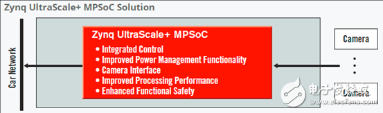
• Quad-core ARM Cortex-A53 for vision analytics, streaming, and automated metadata
• Dual-core ARM Cortex-R5 for real-time peripheral interfaces
• Advanced power management, power islands, and lock-step mode with real-time processing for functional safety
• Video encoder/decoder, supporting H.265/H.264 for display connectivity
• CAN2.0B and Gigabit Ethernet support for IEEE Std 1588 and AVB for in-vehicle communications
应用案例2:
公共安全和军用移动无线电:
• Platform Management Unit (PMU) to dynamically lower power, maximizing battery life
• Quad-core ARM Cortex-A53 to integrate application processing and radio modem
• Vivado HLS and SDx™ Design Environment for high-level (C/C++) waveform development
• W-Mux DSP48 for efficient complex filter implementation
• Processing System (PS) with varying Programmable Logic (PL) for radio scalability with maximum software reuse
• Dedicated configuration security unit (CSU) for security management
Avnet Ultra96™ is an Arm-based, Xilinx ZynqUltraScale+™ MPSoC development board based on the Linaro 96Boards specification.
The Avnet Ultra96 enables hardware and software developers to explore the capabilities of the Zynq® UltraScale+™ MPSoC. Designers can create or evaluate designs for both the Zynq Processor Subsystem (PS) and the Programmable Logic (PL) fabric
图1.Ultra96开发板外形图
Ultra96开发板主要特性:
ZynqUltraScale+ MPSoC ZU3EG SBVA484
Memory
oMicron 2 GB (512M x32) LPDDR4 Memory
oMiroSD Socket
§ Ships with Delkin Utility MLC 16GB card
Wi-Fi / Bluetooth
DisplayPort
1x USB 3.0 Type Micro-B upstream port
2x USB 3.0 Type A downstream ports
40-pin Low-speed expansion header
60-pin High speed expansion header
Mounted on thermal bracket with fan
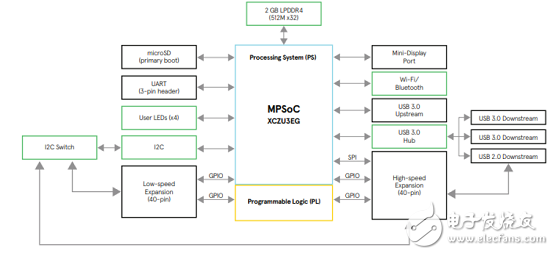
图2.Ultra96开发板框图
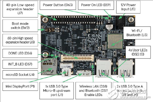
图3.Ultra96开发板拓扑图
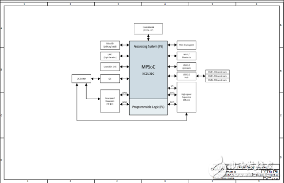
图4.Ultra96开发板电路图(1)
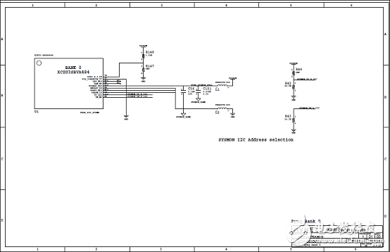
图5.Ultra96开发板电路图(2)
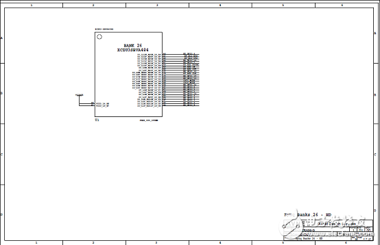
图6.Ultra96开发板电路图(3)
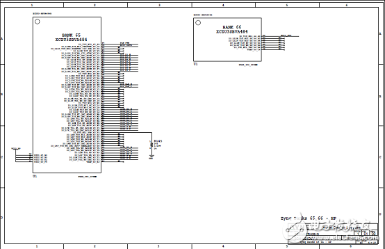
图7.Ultra96开发板电路图(4)
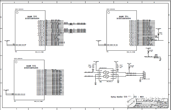
图8.Ultra96开发板电路图(5)
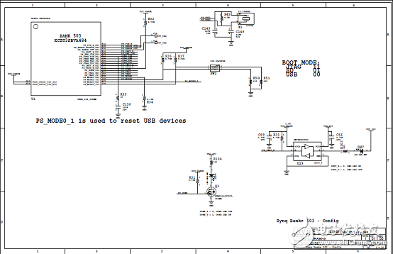
图9.Ultra96开发板电路图(6)
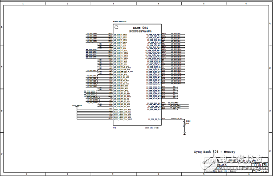
图10.Ultra96开发板电路图(7)
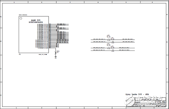
图11.Ultra96开发板电路图(8)
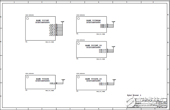
图12.Ultra96开发板电路图(9)
图13.Ultra96开发板电路图(10)
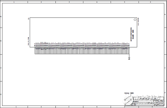
图14.Ultra96开发板电路图(11)
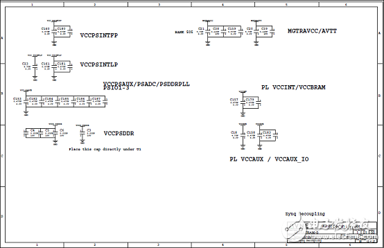
图15.Ultra96开发板电路图(12)
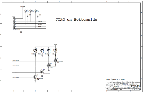
图16.Ultra96开发板电路图(13)
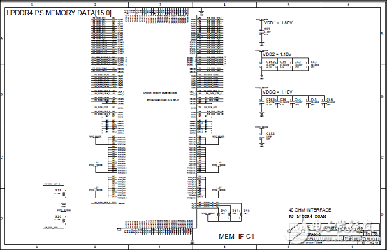
图17.Ultra96开发板电路图(14)
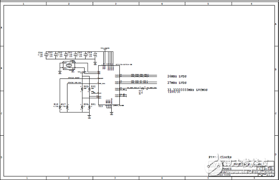
图18.Ultra96开发板电路图(15)
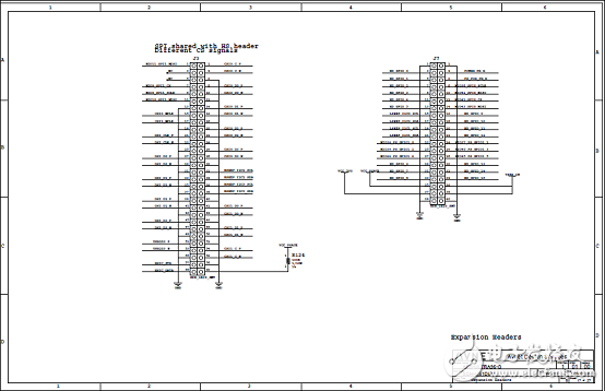
图19.Ultra96开发板电路图(16)
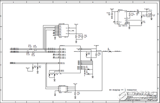
图20.Ultra96开发板电路图(17)
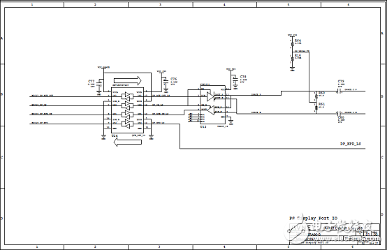
图21.Ultra96开发板电路图(18)
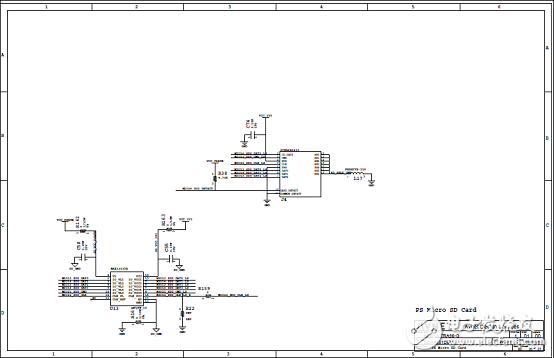
图22.Ultra96开发板电路图(19)
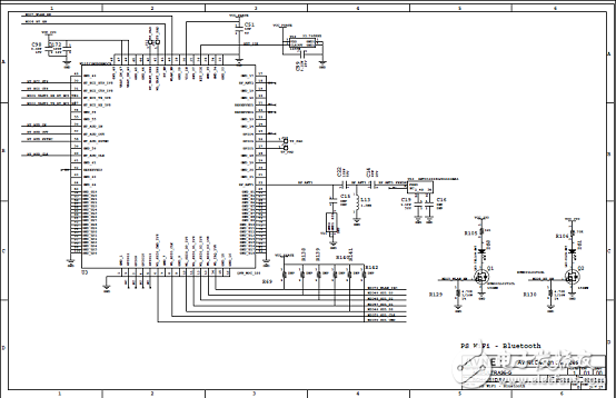
图23.Ultra96开发板电路图(20)
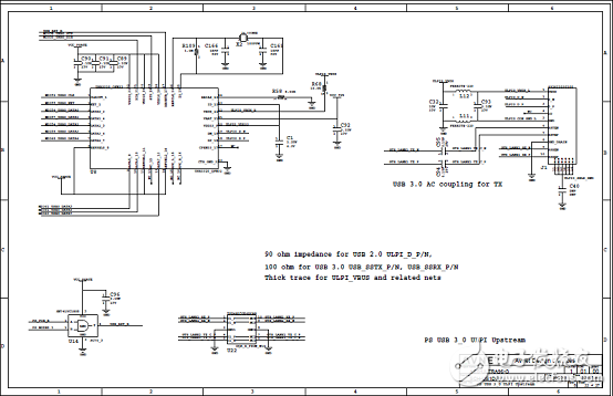
图24.Ultra96开发板电路图(21)
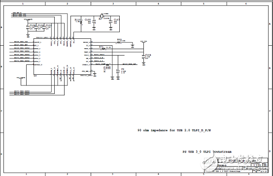
图25.Ultra96开发板电路图(22)
图26.Ultra96开发板电路图(23)
图27.Ultra96开发板电路图(24)
图28.Ultra96开发板电路图(25)
图29.Ultra96开发板电路图(26)
Ultra96开发板材料清单:
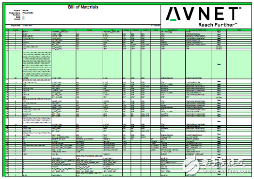
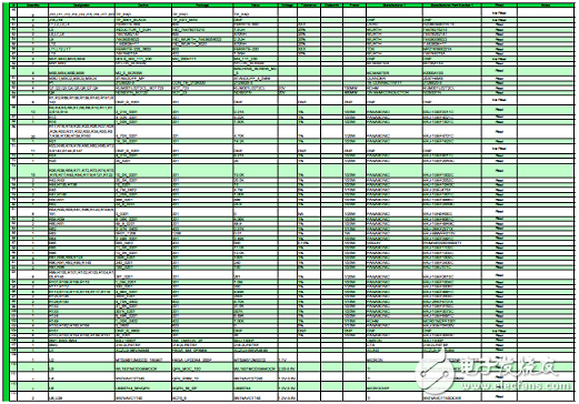
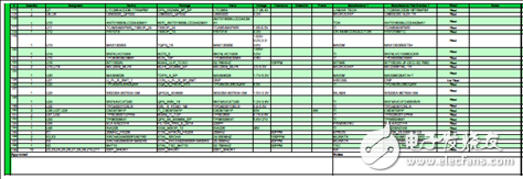
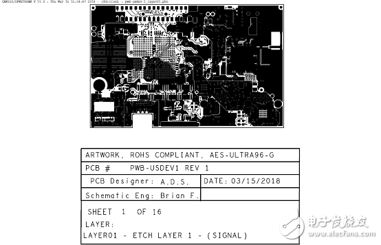
图30.Ultra96开发板PCB设计图(1)

图31.Ultra96开发板PCB设计图(2)
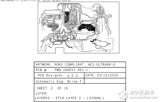
图32.Ultra96开发板PCB设计图(3)
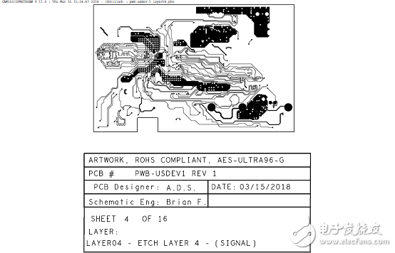
图33.Ultra96开发板PCB设计图(4)
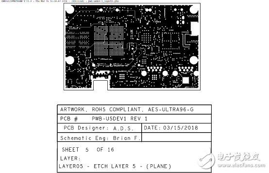
图34.Ultra96开发板PCB设计图(5)
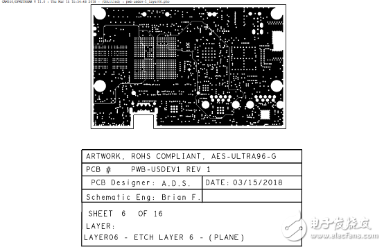
图35.Ultra96开发板PCB设计图(6)
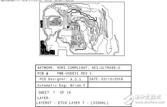
图36.Ultra96开发板PCB设计图(7)
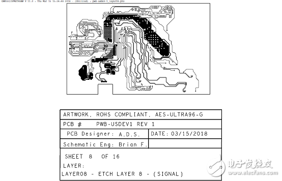
图37.Ultra96开发板PCB设计图(8)
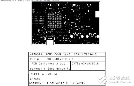
图38.Ultra96开发板PCB设计图(9)
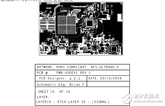
图39.Ultra96开发板PCB设计图(10)
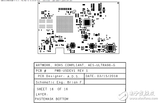
图40.Ultra96开发板PCB设计图(11)
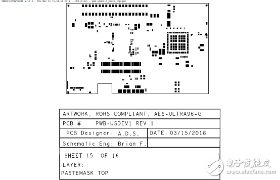
图41.Ultra96开发板PCB设计图(12)
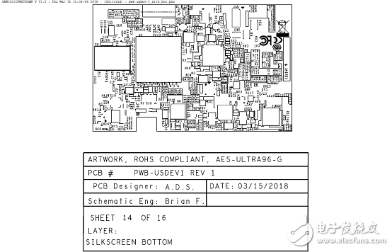
图42.Ultra96开发板PCB设计图(13)
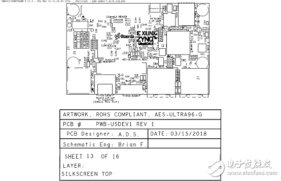
图44.Ultra96开发板PCB设计图(15)
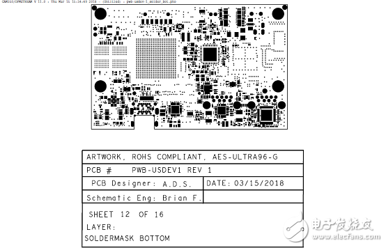
图45.Ultra96开发板PCB设计图(16)
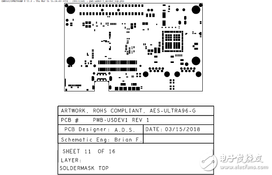
图46.Ultra96开发板PCB设计图(17)
-
Zynq UltraScale + MPSoC USB 3.0 CDC器件类设计2019-01-03 0
-
如何利用ZYNQ MPSoC玩DOOM?2019-10-09 0
-
如何调试Zynq UltraScale+ MPSoC VCU DDR控制器2021-01-07 0
-
ZYNQ Ultrascale+ MPSOC FPGA教程2021-02-02 0
-
Xilinx Zynq UltraScale+ MPSoC系列:逆天性能亮瞎你的双眼2017-02-09 1978
-
Ti推出面向Zynq UltraScale+ MPSoC的电源参考设计2017-03-14 3444
-
Xilinx宣布推出汽车级Zynq UltraScale+ MPSoC系列2018-01-17 9238
-
Xilinx基于ARM的Zynq-7000和Zynq UltraScale+ MPSoC及RFSoC器件是否存在安全漏洞2018-06-28 2519
-
Zynq UltraScale+ MPSoC的发售消息2018-11-27 3308
-
如何调试 Zynq UltraScale+ MPSoC VCU DDR 控制器?2021-02-23 1123
-
米尔电子zynq ultrascale+ mpsoc底板外设资源清单分享2022-01-07 515
-
ZYNQ Ultrascale+ MPSoC系列FPGA芯片设计2022-11-02 1177
-
Zynq UltraScale+ MPSoC的隔离设计示例2023-09-13 142
-
适用于Xilinx Zynq UltraScale+ MPSoC应用的电源参考设计2023-09-13 203
全部0条评论

快来发表一下你的评论吧 !
