

LPC540xx是基于ARM Cortex-M4的32位微控制器
控制/MCU
描述
nxp公司的LPC540xx系列是基于ARM Cortex-M4的32位微控制器,采用3级流水线,具有单独本地指令和数据总线哈佛架构以及用于外设的第三总线,支持分支操作的内部预取单元,处理器工作频率180 MHz,单电源1.71V-3.6V工作,主要用在物联网(IoT)。本文介绍了LPC540xx系列主要特性和优势,框图,以及IoT模块OM40007主要特性,电路图和材料清单。
The LPC540xx is a family of ARM Cortex-M4 based microcontrollers for embedded applications featuring a rich peripheral set with very low power consumption and enhanced debug features.
The ARM Cortex-M4 is a 32-bit core that offers system enhancements such as low power consumption, enhanced debug features, and a high level of support block integration. The ARM Cortex-M4 CPU incorporates a 3-stage pipeline, uses a Harvard architecture with separate local instruction and data buses as well as a third bus for peripherals, andincludes an internal prefetch unit that supports speculative branching. The ARM Cortex-M4 supports single-cycle digital signal processing and SIMD instructions. A hardware floating-point processor is integrated into the core.
The LPC540xx family includes 360 KB of on-chip SRAM, a quad SPI Flash Interface (SPIFI) for expanding program memory, one high-speed and one full-speed USB host and device controller, Ethernet AVB, LCD controller, Smart Card Interfaces, SD/MMC, CAN FD, an External Memory Controller (EMC), a DMIC subsystem with PDM microphone interface and I2S, five general-purpose timers, SCTimer/PWM, RTC/alarm timer, Multi-Rate Timer (MRT), a Windowed Watchdog Timer (WWDT), ten flexible serial communication peripherals (USART, SPI, I2S, I2C interface), Secure Hash Algorithm (SHA), 12-bit 5.0 Msamples/sec ADC, and a temperature sensor.
LPC540xx系列主要特性和优势:
ARM Cortex-M4 core (version r0p1):
ARM Cortex-M4 processor, running at a frequency of up to 180 MHz.
Floating Point Unit (FPU) and Memory Protection Unit (MPU)。
ARM Cortex-M4 built-in Nested Vectored Interrupt Controller (NVIC)。
Non-maskable Interrupt (NMI) input with a selection of sources.
Serial Wire Debug (SWD) with six instruction breakpoints, two literal comparators,and four watch points. Includes Serial Wire Output and ETM Trace for enhancedde bug capabilities, and a debug timestamp counter.
System tick timer.
On-chip memory:
Up to 360 KB total SRAM consisting of 160 KB contiguous main SRAM and an additional 192 KB SRAM on the I&D buses. 8 KB of SRAM bank intended for USB traffic.
General-purpose One-Time Programmable (OTP) memory for user application specific data
ROM API support:
In-Application Programming (IAP) and In-System Programming (ISP)。
ROM-based USB drivers (HID, CDC, MSC, and DFU)。
Supports serial interface booting (UART, I2C, SPI) from an application processor, automated booting from NOR flash (quad SPIFI, 8/16/32-bit external parallel flash),and USB booting (full-speed, high-speed)。
FRO API for selecting FRO output frequency.
OTP API for programming OTP memory.
Random Number Generator (RNG) API.
Execute in place (XIP) from SPIFI NOR flash (in quad, dual SPIFI mode or single-bit SPI mode), and parallel NOR flash.
Serial interfaces:
Flexcomm Interface contains up to 11 serial peripherals. Each Flexcomm Interface(exceptflexcomm 10, which is dedicated for SPI) can be selected by software to bea USART, SPI, or I2C interface. Two Flexcomm Interfaces also include an I2Sinterface. Each Flexcomm Interface includes a FIFO that supports USART, SPI,and I2S if supported by that Flexcomm Interface. A variety of clocking options areavailable to each Flexcomm Interface and include a shared fractional baud-rategenerator.
I2C-bus interfaces support Fast-mode and Fast-mode Plus with data rates of up to 1Mbit/s and with multiple address recognition and monitor mode. Two sets of trueI2C pads also support High Speed Mode (3.4 Mbit/s) as a slave.
Two ISO 7816 Smart Card Interfaces with DMA support.
USB 2.0 high-speed host/device controller with on-chip high-speed PHY.
USB 2.0 full-speed host/device controller with on-chip PHY and dedicated DMA controller supporting crystal-less operation in device mode using software library.
SPIFI with XIP feature uses up to four data lines to access off-chip SPI/DSPI/QSPI flash memory at a much higher rate than standard SPI or SSP interfaces.
Ethernet MAC with MII/RMII interface with Audio Video Bridging (AVB) support and dedicated DMA controller.
Two CAN FD modules with dedicated DMA controller.
Digital peripherals:
DMA controller with 32 channels and up to 24 programmable triggers, able to access all memories and DMA-capable peripherals.
LCD Controller supporting both Super-Twisted Nematic (STN) and Thin-Film Transistor (TFT) displays. It has a dedicated DMA controller, selectable display resolution (up to 1024 x 768 pixels), and supports up to 24-bit true-color mode.
External Memory Controller (EMC) provides support for asynchronous static memory devices such as RAM, ROM and flash, in addition to dynamic memories such as single data rate SDRAM with an SDRAM clock of up to 100 MHz. EMC bus width (bit) on TFBGA180, TFBGA100, and LQFP100 packages supports up to 8/16 data line wide static memory.
Secured digital input/output (SD/MMC and SDIO) card interface with DMA support.
CRC engine block can calculate a CRC on supplied data using one of three standard polynomials with DMA support.
Up to 171 General-Purpose Input/Output (GPIO) pins.
GPIO registers are located on the AHB for fast access. The DMA supports GPIO ports.
Up to eight GPIOs can be selected as Pin Interrupts (PINT), triggered by rising,falling or both input edges.
Two GPIO Grouped Interrupts (GINT) enable an interrupt based on a logical(AND/OR) combination of input states.
Analog peripherals:
12-bit ADC with 12 input channels and with multiple internal and external trigger inputs and sample rates of up to 5.0 MSamples/sec. The ADC supports two independent conversion sequences.
Integrated temperature sensor connected to the ADC.
DMIC subsystem includes a dual-channel PDM microphone interface with decimators,filtering, and hardware voice activity detection. The processed output data can berouted directly to an I2S interface if needed.
Timers:
Five 32-bit general purpose timers/counters. All five timers support up to fourcapture inputs and four compare outputs, PWM mode, and external count input.Specific timer events can be selected to generate DMA requests.
One SCTimer/PWM with eight input and ten output functions (including capture and match)。 Inputs and outputs can be routed to or from external pins and internally toor from selected peripherals. Internally, the SCTimer/PWM supports 16match/captures, 16 events, and 16 states.
32-bit Real-time clock (RTC) with 1 s resolution running in the always-on powerdomain. A timer in the RTC can be used for wake-up from all low power modesincluding deep power-down, with 1 ms resolution.
Multiple-channel multi-rate 24-bit timer (MRT) for repetitive interrupt generation atup to four programmable, fixed rates.
Windowed Watchdog Timer (WWDT)。
Repetitive Interrupt Timer (RIT) for debug time stamping and for general purposeuse.
Security features:
Secure Hash Algorithm (SHA1/SHA2) module supports boot with dedicated DMA controller.
Clock generation:
12 MHz internal Free Running Oscillator (FRO)。 This oscillator provides aselectable 48 MHz or 96 MHz output, and a 12 MHz output (divided down from theselected higher frequency) that can be used as a system clock. The FRO istrimmed to 1 % accuracy over the entire voltage and temperature range.
Crystal oscillator with an operating range of 1 MHz to 25 MHz.
Watchdog Oscillator (WDTOSC) with a frequency range of 6 kHz to 1.5 MHz.
32.768 kHz low-power RTC oscillator.
System PLL allows CPU operation up to the maximum CPU rate and can run from the main oscillator, the internal FRO, the watchdog oscillator or the 32.768 KHz RTC oscillator.
Two additional PLLs for USB clock and audio subsystem.
Independent clocks for the SPIFI interface, ADC, USBs, and the audio subsystem.
Clock output function with divider.
Frequency measurement unit for measuring the frequency of any on-chip oroff-chip clock signal.
Power control:
Programmable PMU (Power Management Unit) to minimize power consumption and to match requirements at different performance levels.
Reduced power modes: sleep, deep-sleep, and deep power-down.
Wake-up from deep-sleep modes due to activity on the USART, SPI, and I2C peripherals when operating as slaves.
Ultra-low power Micro-tick Timer, running from the Watchdog oscillator that can be used to wake up the device from low power modes.
Power-On Reset (POR)。
Brown-Out Detect (BOD) with separate thresholds for interrupt and forced reset.
Single power supply 1.71 V to 3.6 V.
Power-On Reset (POR)。
Brown-Out Detect (BOD) with separate thresholds for interrupt and forced reset.
JTAG boundary scan supported.
128 bit unique device serial number for identification.
Operating temperature range 40℃ to +105℃。
Available in TFBGA180, TFBGA100, LQFP208, and LQFP100 packages.
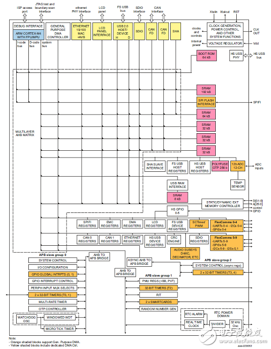
图1.LPC540xx系列框图
LPC54018 IoT模块OM40007
OM40007: LPC54018 IoT Module for the LPC540xx family of MCUs
The LPC54018 IoT module, developed by NXP in partnership with Embedded Artists, is self-contained, high performance, IEEE802.11 enabled microcontroller module for the development of products utilizing Amazon FreeRTOS or other IoT platforms. The module can be used as a standalone or plugged into a motherboard or baseboard for rapid product development and prototyping.
The IoT module baseboard (part number OM40006) is jointly developed by NXP and Embedded Artists. It provides several on-board peripherals for rapid prototyping and evaluation. The on-board peripherals include SDRAM, LCD with touchscreen, audio CODEC, digital microphone, Ethernet PHY, micro SD card slot and Arduino UNO expansion connectors. The baseboard also includes an on-board debug probe. See or visit for more information on this board.
图2.IoT模块OM40007外形图
IoT模块OM40007主要特性:
• Amazon FreeRTOS enabled, ready for use in designs powered by AWS
•LPC54018 power-efficient Microcontroller Units (MCUs) with advanced peripheralsbased on Arm® Cortex®-M4 Core, running at 180 MHz
• High speed USB device port
• Longsys IEEE802.11b/g/n module based on Qualcomm GT1216
• Macronix 128 Mb flash (MX25L12835FM2)
• User LED
• External debug probe connector can be used to connect NXP (LPC-Link2), SEGGER,P&E Micro, and other popular ARM Cortex compatible probes
• Reset button
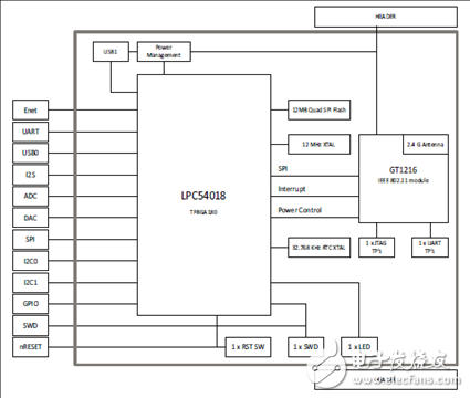
图3.IoT模块OM40007框图
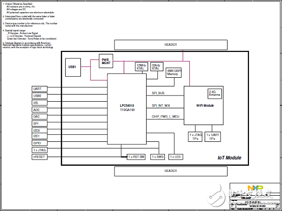
图4.IoT模块OM40007电路图(1)
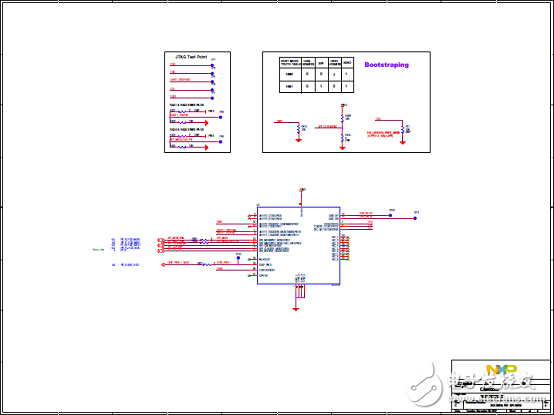
图5.IoT模块OM40007电路图(2)
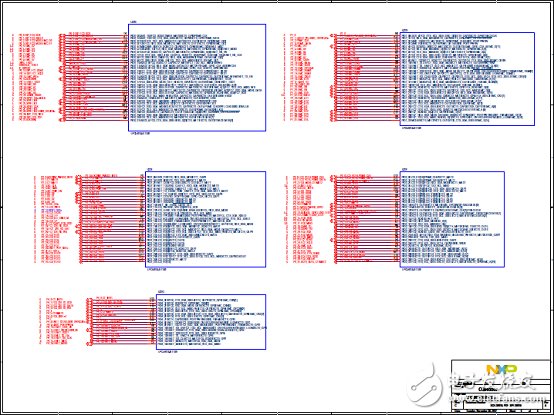
图6.IoT模块OM40007电路图(3)
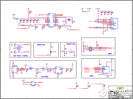
图7.IoT模块OM40007电路图(4)
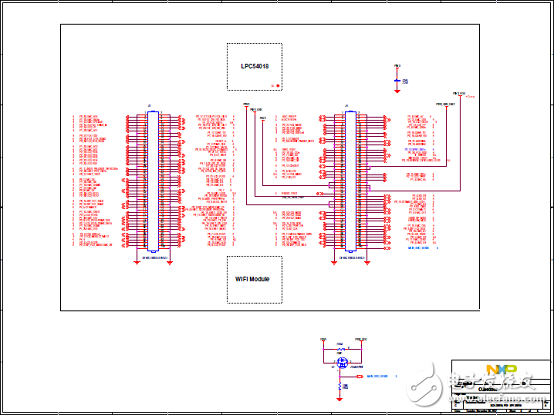
图8.IoT模块OM40007电路图(5)
IoT模块OM40007材料清单见:
BOM-30019_A.xls
详情请见:
https://www.nxp.com/docs/en/data-sheet/LPC540xx.pdf
和https://www.nxp.com/docs/en/user-guide/UM11078.pdf
LPC540xx.pdf
-
ARM Cortex-M4控制开发2013-07-28 0
-
恩智浦 NXP ARM7 ARM9 Cortex-M0 M3 M4 内核芯片汇总2014-10-13 0
-
ARM Cortex-M4内核MCU的优势在哪里2015-02-13 0
-
图书推荐:《ARM Cortex-M4微控制器原理与应用:基于Atmel SAM4系列》2016-06-12 0
-
什么是用于数字信号控制的CORTEX-M4处理器?2019-09-25 0
-
基于ARM cortex-M4内核的STM32F303VET6微控制器2020-07-20 0
-
基于ARM Cortex-M4内核的STM32F429线路微控制器2020-08-19 0
-
基于Arm®Cortex®-M0+内核的32位微控制器2022-11-24 0
-
具有Cortex-M4和Cortex-M0的不对称双核数字信号控制器2022-12-06 0
-
LPC540xx使用指南2022-12-07 0
-
LPC540xx MCU相关资料分享2022-12-07 0
-
LPC43xx/LCP43Sxx ARM Cortex-M4/M0多核微控制器资料分享2022-12-07 0
-
LPC18xx ARM Cortex-M3微控制器相关资料分享2022-12-07 0
-
恩智浦推出基于Cortex-M0微控制LPC1100微控制器2009-11-18 1229
-
恩智浦ARM Cortex-M3 USB微控制器LPC1342009-12-14 1191
全部0条评论

快来发表一下你的评论吧 !
