

Cypress MB9B520M 32位ARM MCU开发方案
嵌入式技术
描述
cypress公司的MB9B520M是高度集成的32位MCU,基于Arm® Cortex®-M3处理器,工作频率高达72MHz,集成了片上闪存和SRAM,以及外设功能如各种计时器,ADC,DAC和通信接口如USB, CAN, UART, CSIO, I2C, LIN,主要用在嵌入式应用和低成本低功耗应用.本文介绍了MB9B520M主要特性,框图以及评估板SK-FM3-80PMC-MB9BF524M主要特性,电路图和主要元件分布图.
The MB9B520M Series are highly integrated 32-bit microcontrollers dedicated for embedded controllers with low-power consumption mode and competitive cost.
These series are based on the Arm® Cortex®-M3 Processor with on-chip Flash memory and SRAM, and have peripheral functions such as various timers, ADCs, DACs and Communication Interfaces (USB, CAN, UART, CSIO, I2C, LIN).
The products which are described in this data sheet are placed into TYPE9 product categories in “FM3 Family Peripheral Manual”.
MB9B520M主要特性:
32-bit Arm® Cortex®-M3 Core
Processor version: r2p1
Up to 72 MHz frequency Operation
Integrated Nested Vectored Interrupt Controller (NVIC): 1
NMI(non-maskable interrupt) and 48 peripheral interruptsand 16 priority levels
24-bit System timer (Sys Tick): System timer for OS taskmanagement
On-chip Memories
[Flash memory]
Dual operation Flash memory
Dual Operation Flash memory has the upper bank and thelower bank.
So,this series could implement erase, write and readoperations for each bank simultaneously.
Main area: Up to 256 Kbytes (Up to 240 Kbytes upper bank+ 16 Kbytes lower bank)
Work area: 32 Kbytes (lower bank)
Read cycle: 0 wait-cycle
Security function for code protection
[SRAM]
This Series on-chip SRAM is composed of two independent
SRAM (SRAM0, SRAM1). SRAM0 is connected to I-code busand D-code bus of Cortex-M3 core. SRAM1 is connected toSystem bus.
SRAM0: Up to 16 Kbytes
SRAM1: Up to 16 Kbytes
USB Interface
The USB interface is composed of Device and Host.
PLL for USB is built-in, USB clock can be generated bymultiplication of Main clock.
[USB device]
USB2.0 Full-Speed supported
Max 6 EndPoint supported
EndPoint 0 is control transfer
EndPoint 1, 2 can select Bulk-transfer, Interrupt-transfer orIsochronous-transfer
EndPoint 3 to 5 can select Bulk-transfer orInterrupt-transfer
EndPoint 1 to 5 are comprised of Double Buffers.
The size of each endpoint is according to the follows.
• Endpoint 0, 2 to 5: 64 bytes
• Endpoint 1: 256 bytes
[USB host]
USB2.0 Full/Low-speed supported
Bulk-transfer, interrupt-transfer and Isochronous-transfersupport
USB Device connected/dis-connected automatic detection
Automatic processing of the IN/OUT token handshakepacket
Max 256-byte packet-length supported
Wake-up function supported
CAN Interface
Compatible with CAN Specification 2.0A/B
Maximum transfer rate: 1 Mbps
Built-in 32 message buffer
Multi-function Serial Interface (Max eight channels)
4 channels with 16 steps×9-bit FIFO (ch.0/1/3/4), 4 channelswithout FIFO (ch.2/5/6/7)
Operation mode is selectable from the followings for eachchannel.
UART
CSIO
LIN
I2C
[UART]
Full duplex double buffer
Selection with or without parity supported
Built-in dedicated baud rate generator
External clock available as a serial clock
Hardware Flow control: Automatically control thetransmission/reception by CTS/RTS (only ch.4)
Various error detection functions available (parity errors,framing errors, and overrun errors)
[CSIO]
Full duplex double buffer
Built-in dedicated baud rate generator
Overrun error detection function available
[LIN]
LIN protocol Rev.2.1 supported
Full duplex double buffer
Master/Slave mode supported
LIN break field generation (can be changed to 13 to 16-bitlength)
LIN break delimiter generation (can be changed to 1 to 4-bitlength)
Various error detection functions available (parity errors,framing errors, and overrun errors)
[I2C]
Standard mode (Max 100 kbps) / Fast mode (Max 400 kbps)supported
DMA Controller (Eight channels)
The DMA Controller has an independent bus from the CPU, soCPU and DMA Controller can process simultaneously.
8 independently configured and operated channels
Transfer can be started by software or request from thebuilt-in peripherals
Transfer address area: 32-bit (4 Gbytes)
Transfer mode: Block transfer/Burst transfer/Demandtransfer
Transfer data type: byte/half-word/word
Transfer block count: 1 to 16
Number of transfers: 1 to 65536
A/D Converter (Max 26 channels)
[12-bit A/D Converter]
Successive Approximation type
Built-in 2 units
Conversion time: 0.8 μs @ 5 V
Priority conversion available (priority at 2 levels)
Scanning conversion mode
Built-in FIFO for conversion data storage (for SCANconversion: 16 steps, for Priority conversion:4 steps)
D/A Converter (Max two channels)
R-2R type
10-bit resolution
Base Timer (Max eight channels)
Operation mode is selectable from the followings for eachchannel.
16-bit PWM timer
16-bit PPG timer
16-/32-bit reload timer
16-/32-bit PWC timer
General-Purpose I/O Port
This series can use its pins as general-purpose I/O ports whenthey are not used for peripherals. Moreover, the port relocatefunction is built in. It can set which I/O port the peripheralfunction can be allocated to.
Capable of pull-up control per pin
Capable of reading pin level directly
Built-in the port relocate function
Up to 65 high-speed general-purpose I/O Ports@80pinPackage
Some ports are 5V tolerant.
See “List of Pin Functions” and “I/O Circuit Type” to confirmthe corresponding pins.
Dual Timer (32-/16-bit Down Counter)
The Dual Timer consists of two programmable 32-/16-bit downcounters.
Operation mode is selectable from the followings for eachchannel.
Free-running
Periodic (=Reload)
One-shot
Quadrature Position/Revolution Counter (QPRC)(Max two channels)
The Quadrature Position/Revolution Counter (QPRC) is usedto measure the position of the position encoder. Moreover, it ispossible to use as the up/down counter.
The detection edge of the three external event input pins AIN,BIN and ZIN is configurable.
16-bit position counter
16-bit revolution counter
Two 16-bit compare registers
Multi-function Timer
The Multi-function timer is composed of the following blocks.
16-bit free-run timer × 3 ch./unit
Input capture × 4 ch./unit
Output compare × 6 ch./unit
A/D activation compare × 2 ch./unit
Waveform generator × 3 ch./unit
16-bit PPG timer × 3 ch./unit
The following function can be used to achieve the motorcontrol.
PWM signal output function
DC chopper waveform output function
Dead time function
Input capture function
A/D convertor activate function
DTIF (Motor emergency stop) interrupt function
Real-time clock (RTC)
The Real-time clock can countYear/Month/Day/Hour/Minute/Second/A day of the week from00 to 99.
The interrupt function with specifying date and time
(Year/Month/Day/Hour/Minute) is available. This function isalso available by specifying only Year, Month, Day, Hour orMinute.
Timer interrupt function after set time or each set time.
Capable of rewriting the time with continuing the time count.
Leap year automatic count is available.
Watch Counter
The Watch counter is used for wake up from Sleep and Timermode.
Interval timer: up to 64 s (Max) @ Sub Clock: 32.768 kHz
External Interrupt Controller Unit
Up to 23 external interrupt input pins @ 80 pin Package
Include one non-maskable interrupt (NMI) input pin
Watchdog Timer (Two channels)
A watchdog timer can generate interrupts or a reset when atime-out value is reached.
This series consists of two different watchdogs, a "Hardware"watchdog and a "Software" watchdog.
The "Hardware" watchdog timer is clocked by the built-inLow-speed CR oscillator. Therefore, the "Hardware" watchdogis active in any low-power consumption modes except RTC,Stop, Deep Standby RTC, Deep Standby Stop modes.
CRC (Cyclic Redundancy Check) Accelerator
The CRC accelerator calculates the CRC which has a heavysoftware processing load, and achieves a reduction of theintegrity check processing load for reception data and storage.
CCITT CRC16 and IEEE-802.3 CRC32 are supported.
CCITT CRC16 Generator Polynomial: 0x1021
IEEE-802.3 CRC32 Generator Polynomial: 0x04C11DB7
Clock and Reset
[Clocks]
Selectable from five clock sources (2 external oscillators, 2built-in CR oscillators, and Main PLL).
Main Clock: 4 MHz to 48 MHz
Sub Clock: 32.768 kHz
Built-in High-speed CR Clock: 4 MHz
Built-in Low-speed CR Clock: 100 kHz
Main PLL Clock
[Resets]
Reset requests from INITX pin
Power-on reset
Software reset
Watchdog timers reset
Low-voltage detection reset
Clock Super Visor reset
Clock Super Visor (CSV)
Clocks generated by built-in CR oscillators are used tosupervise abnormality of the external clocks.
If external clock failure (clock stop) is detected, reset isasserted.
If external frequency anomaly is detected, interrupt or reset isasserted.
Low-Voltage Detector (LVD)
This Series includes 2-stage monitoring of voltage on the VCCpins. When the voltage falls below the voltage that has beenset, Low-Voltage Detector generates an interrupt or reset.
LVD1: error reporting via interrupt
LVD2: auto-reset operation
Low-Power Consumption Mode
Six low-power consumption modes supported.
Sleep
Timer
RTC
Stop
Deep Standby RTC (selectable between keeping the value ofRAM and not)
Deep Standby Stop (selectable between keeping the value ofRAM and not)
Debug
Serial Wire JTAG Debug Port (SWJ-DP)
Unique ID
Unique value of the device (41 bits) is set.
Power Supply
Wide range voltage:
VCC = 2.7 V to 5.5 V
USBVCC = 3.0 V to 3.6 V (when USB is used)
= 2.7 V to 5.5 V (when GPIO is used)
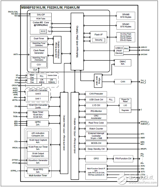
图1.MB9B520M框图
评估板SK-FM3-80PMC-MB9BF524M
Supports CY9B120M, CY9B320M and CY9B520M Series
The SK-FM3-80PMC-MB9BF524M includes a low-cost evaluation board based on the Spansion FM3 microcontroller MB9B520M Series.
SK-FM3-80PMC-9BF524M-JL includes a low-cost evaluation board based on the Spansion FM3 microcontroller MB9B520M Series and the JTAG adapter J-Link
评估板SK-FM3-80PMC-MB9BF524M主要特性:
Features of the SK-FM3-80PMC-MB9BF524M board: Microcontroller MB9BF524M
1x UART-Transceiver (SUB-D9 connector)
1x USB to serial converter (Type-B connector)
1x High-speed CAN-Transceiver (SUB-D9 connector)
1x USB-Host (Type-A connector)
1x USB-Device (Type-B connector)
2x LED-Display (7-Segment)
2x ‘User’-button
1x ‘Reset’-button,‘Reset’-LED
JTAG-Interface on a 20 pin-header
FMtouch connector interface for software touch solutions
TSC-Interface to connect for example the Spansion SK-TSC-1127S-SB
All 80 pins routed to pin-header
On-board 5V and 3V voltage regulators, ‘Power’-LED
Power supply via USB (UART’B’), USB-Device, JTAG or external with a 8V to 12V power connector
图2.评估板SK-FM3-80PMC-MB9BF524M外形图
评估板SK-FM3-80PMC-MB9BF524M包括:
The SK-FM3-80PMC-MB9BF524M contains SK-FM3-80PMC-MB9BF524M evaluation board with MB9BF524M
USB cable
DVD: Documentation, USB driver, Software examples, Programmer
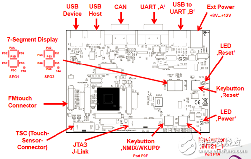
图3.评估板SK-FM3-80PMC-MB9BF524M主要元件分布图
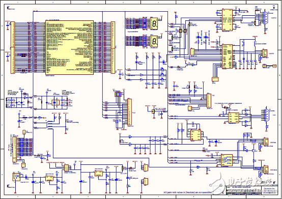
图4.评估板SK-FM3-80PMC-MB9BF524M电路图
- 相关推荐
- Cypress
-
FM3 CY9BFx1xS/T系列Arm Cortex-M3微控制器Cypress2024-02-26 0
-
新唐科技在16个城市举办 NuMicro™ Family ARM® Cortex™-M0/M4 32位...2013-11-19 0
-
恩智浦 NXP ARM7 ARM9 Cortex-M0 M3 M4 内核芯片汇总2014-10-13 0
-
Cypress PSoC蓝牙低功耗开发设计攻略2015-05-08 0
-
MB9BF524K可以使用32MHz晶振的FLASH MCU编程器吗?2018-12-21 0
-
TWR-K64F120M是Kinetis K24,K63和K64 120 MHz 32位ARM Cortex-M4 MCU的开发板2019-08-12 0
-
赛普拉斯Cypress PSoC 6 MCU简介及常见4款开发套件工具板2019-12-10 0
-
如何选择8位MCU和32位MCU架构的指南使用?2021-03-01 0
-
谈谈基于ARM Cortex M0国产32位单片机MM32SPIN220B2021-07-21 0
-
基于ARM架构的MCU选择2021-11-10 0
-
以ARM为主的32位MCU2021-11-23 0
-
Arm 10款 Cortex-M系列MCU内核对比2022-07-29 0
-
干货:对比看看Arm推出的10款Cortex-M系列MCU内核IP2022-07-29 0
-
国内MCU厂商90%都采用的Arm 的Cortex-M系列内核,优点在哪?2022-07-29 0
-
【野火启明6M5开发板体验】野火启明开发板和瑞萨RA MCU介绍2022-12-14 0
全部0条评论

快来发表一下你的评论吧 !
