

基于ADF4371集成VCO的微波宽带合成器解决方案
电子说
描述
ADI公司的ADF4371是集成压控振荡器(VCO)的微波宽带合成器,其基本输出频率范围从4000MHz到800MHz,和外接大回路滤波器和外接基准频率一起,可产生62.5MHz到32GHz的输出频率,高分辨率39位分数模块,典型的杂散为-90dBc,集成的rms抖动为38 fs(1 kHz to 100 MHz),归一化相位噪声图为−234 dBc/Hz PFD@ 250 MHz,基准频率工作600MHz,可编分频器1,2,4,8,16, 32或64输出,模拟和数字电源3.3V,VCO电源3.3V和5V,主要用在无线基础设备(移动通信(MC-GSM)的多载波全球系统,5G),测试测量,航天与国防,时钟发生器。本文介绍了ADF4371主要特性,功能框图以及评估板EV-ADF4371SD2Z主要特性,建立图,电路图,材料清单和PCB设计图。
The ADF4371 allows implementation of fractional-N or Integer N phase-locked loop (PLL) frequency synthesizers when used with an external loop filter and an external reference frequency. The wideband microwave voltage controlled oscillator (VCO) design allows frequencies from 62.5 MHz to 32 GHz to be generated. The ADF4371 has an integrated VCO with a fundamental output frequency ranging from 4000 MHz to 8000 MHz. In addition, the VCO frequency is connected to divide by 1,2,4,8,16,32,or 64 circuits that allows the user to generate radio frequency (RF) output frequencies as low as 62.5 MHz at RF8x. A frequency multiplier at RF16x generates from 8 GHz to 16 GHz. A frequency quadrupler generates frequencies from 16 GHz to 32 GHz at RF32x. RFAUX8x duplicates the frequency range of RF8x or permits direct access to the VCO output. To suppress the unwanted products of frequency multiplication, a harmonic filter exists between the multipliers and the output stages of RF16x and RF32x. Control of all on-chip registers is through a 3-wire interface. The ADF4371 operates with analog and digital power supplies ranging from 3.15 V to 3.45 V, and 5 V for the VCO power supply. The ADF4371 also contains hardware and software power-down modes.
ADF4371主要特性:
RF output frequency range: 62.5 MHz to 32,000 MHz
Fractional-N synthesizer and Integer N synthesizer
High resolution 39-bit fractional modulus
Typical spurious PFD: −90 dBc
Integrated rms jitter: 38 fs (1 kHz to 100 MHz)
Normalized phase noise floor: −234 dBc/Hz PFD operation to 250 MHz
Reference frequency operation to 600 MHz
Programmable divide by 1,2,4,8,16,32,or64 output
62.5 MHz to 8,000 MHz output at RF8x and RFAUX8x
8,000 MHz to 16,000 MHz output at RF16x
16,000 MHz to 32,000 MHz output at RF32x
Lock time approximately 3 ms with automatic calibration
Lock time 《30 μs with autocalibration bypassed
Analog and digital power supplies: 3.3 V
VCO power supply: 3.3 V and 5 V
RF output mute function
7mm×7mm, 48-terminal LGA package
ADF4371应用:
Wireless infrastructure (multicarrier global system for mobile communication (MC-GSM), 5 G)
Test equipment and instrumentation
Clock generation
Aerospace and defense
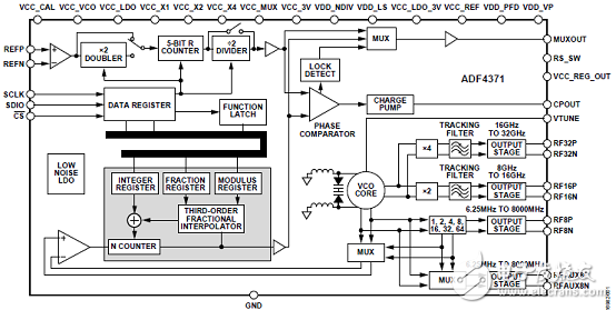
图1.ADF4371功能框图
评估板EV-ADF4371SD2Z
图2.评估板EV-ADF4371SD2Z外形图
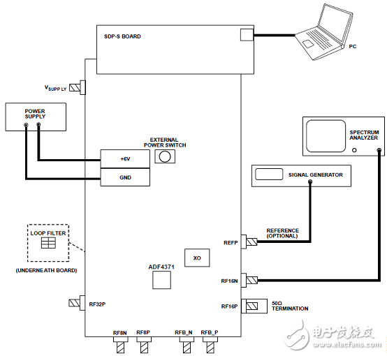
图3.评估板EV-ADF4371SD2Z建立图
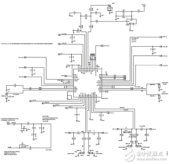
图4.评估板EV-ADF4371SD2Z电路图(1)
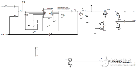
图5.评估板EV-ADF4371SD2Z电路图(2)
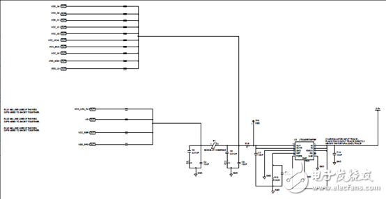
图6.评估板EV-ADF4371SD2Z电路图(3)
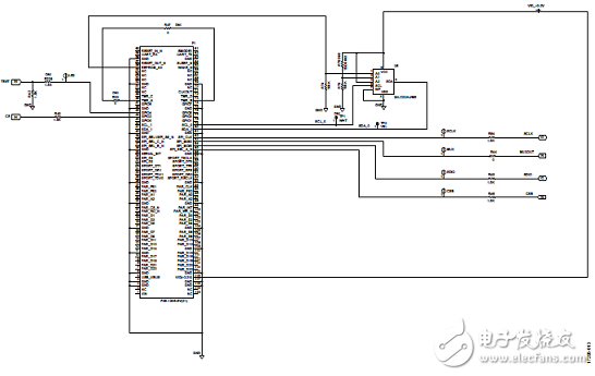
图7.评估板EV-ADF4371SD2Z电路图(4)
评估板EV-ADF4371SD2Z材料清单:
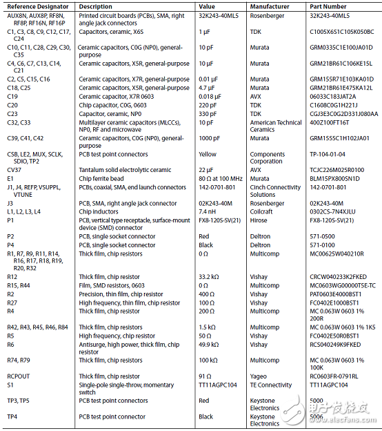
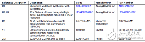
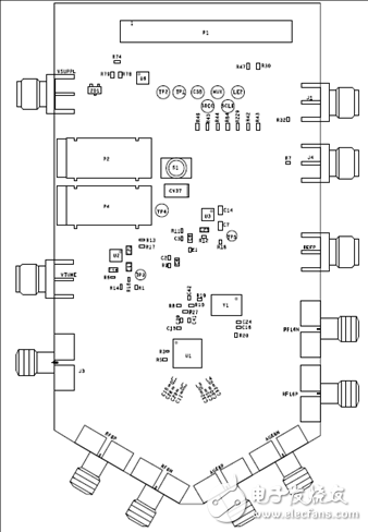
图8.评估板EV-ADF4371SD2Z PCB设计图(1):顶层,丝印
图9.评估板EV-ADF4371SD2Z PCB设计图(2): 底层,丝印
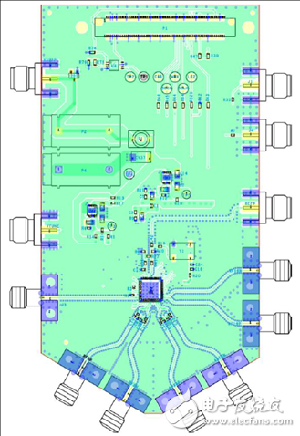
图10.评估板EV-ADF4371SD2Z PCB设计图(3):层1,基层
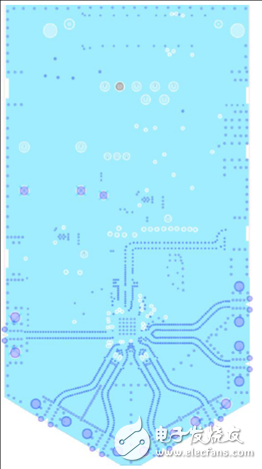
图11.评估板EV-ADF4371SD2Z PCB设计图(4):层2,地
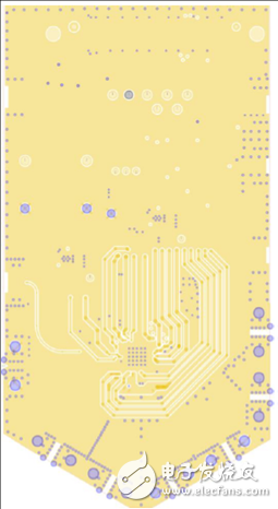
图12.评估板EV-ADF4371SD2Z PCB设计图(5):层3,电源
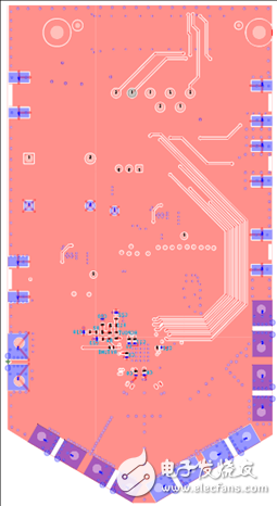
图13.评估板EV-ADF4371SD2Z PCB设计图(6):层4,次面
-
ADF4377 微波宽带合成器和集成VCO数据表 ADI2023-10-11 69
-
ADF4368:微波宽带合成器和集成VCO数据表 ADI2023-10-10 66
-
ADI推新款频率合成器ADF4371 支持各种射频/微波系统设计2018-06-05 9190
-
ADF4371 带集成 VCO 的微波宽带合成器2019-02-22 1200
-
贸泽电子发布Analog Devices ADF437x合成器2019-11-18 1169
-
集成压控振荡器数据表的微波宽带合成器ADF53552021-04-14 458
-
集成压控振荡器数据表的微波宽带合成器ADF43722021-04-22 557
-
集成压控振荡器数据表的微波宽带合成器ADF43552021-04-23 518
-
集成压控振荡器数据表的微波宽带合成器ADF4355-32021-04-28 419
-
UG-805:集成压控振荡器的ADF4355微波宽带合成器评估2021-05-09 425
-
UG-1548:评估集成压控振荡器的ADF4372微波宽带合成器2021-05-12 389
-
UG-1474:评估集成压控振荡器的ADF4371微波宽带合成器2021-05-16 395
-
集成压控振荡器数据表的微波宽带合成器ADF53562021-05-20 460
-
UG-1062:评估集成压控振荡器的ADF4356微波宽带合成器2021-05-22 403
-
CDF5356: 微波宽带合成器和集成 VCO 数据表 ADI2023-10-10 14
全部0条评论

快来发表一下你的评论吧 !
