

ATSAME70Q21的主要特性以及电路图
电子说
描述
Microchip公司的ATSAME70Q21是基于32位ARM Cortex-M7处理器和浮点单元(FPU)的闪存微控制器系列产品,工作频率高达300MHz,具有多达2048KB闪存,多达384KB多端口SRAM,以及可配置指令和数据紧密耦合存储器,加强DSP内核功能,同时具有多种网络/连接外设,包括CAN-FD接口和10/100Mbps以太网MAC和特别的支持音视频桥接器(AVB);其它通信接口包括HS USB主和设备,HSSDCard/SDIO/MMC接口,USART,SPI和多个TWI.模拟特性包括两个2Msps 12位ADC,2Msps 12位DAC.主要用在物联网(IoT),可穿戴,数字音频,汽车电子,马达控制,计量和连接。本文介绍了ATSAME70Q21主要特性,SAM S70, SAM E70, V70和V71 144引脚框图,以及SAM E70 Xplained Ultra评估板DM320113主要特性,框图,电路图,材料清单和PCB设计图。
The Microchip SAME70Q21 devices are members of a flash microcontrollers family based on the high-performance 32-bit ARM Cortex-M7 processor with Floating Point Unit (FPU)。 These devices operate at up to 300MHz and feature up to 2048 Kbytes of Flash, up to 384 Kbytes of multi-port SRAM and configurable Instruction and Data Tightly Couple Memories to leverage the advanced DSP capabilities of the core. SAME70Q21 features multiple networking/connectivity peripherals, including CAN-FD interface and one 1O/100Mbps Ethernet MAC with specific hardware support for Audio Video Bridging (AVB)。 Additional communication interfaces include a HS USB Host and Device, a HS SDCard/SDIO/MMC interface, USARTs, SPIs and multiple TWIs. Analog features include dual 2Msps 12-bit ADCs with analog front end offering offset and gain error correction, and 2Msps 12-bit DAC.
The SAME70Q21 is available in 144-pin QFP and BGA package options.
ATSAME70Q21主要特性:
Core
• ARM® Cortex®-M7 running at up to 300 MHz
• 16 Kbytes of I-Cache and 16 Kbytes of D-Cache with Error Code Correction (ECC)
• Single-precision and double-precision HW Floating Point Unit (FPU)
• Memory Protection Unit (MPU) with 16 zones
• DSP Instructions, Thumb®-2 Instruction Set
• Embedded Trace Module (ETM) with instruction trace stream, including Trace Port Interface Unit(TPIU)
Memories
• Up to 2048 Kbytes embedded Flash with unique identifier and user signature for user-defined data
• Up to 384 Kbytes embedded Multi-port SRAM
• Tightly Coupled Memory (TCM)
• 16 Kbytes ROM with embedded Bootloader routines (UART0, USB) and IAP routines
• 16-bit Static Memory Controller (SMC) with support for SRAM, PSRAM, LCD module, NOR andNAND Flash with on-the-fly scrambling
• 16-bit SDRAM Controller (SDRAMC) interfacing up to 256 MB and with on-the-fly scrambling
System
• Embedded voltage regulator for single-supply operation
• Power-on-Reset (POR), Brown-out Detector (BOD) and Dual Watchdog for safe operation
• Quartz or ceramic resonator oscillators: 3 MHz to 20 MHz main oscillator with failure detection, 12MHz or 16 MHz needed for USB operations. Optional low-power 32.768 kHz for RTC or device clock
• RTC with Gregorian calendar mode, waveform generation in low-power modes
• RTC counter calibration circuitry compensates for 32.768 kHz crystal frequency variations
• 32-bit low-power Real-time Timer (RTT)
• High-precision Main RC oscillator with 12 MHz default frequency.
• 32.768 kHz crystal oscillator or Slow RC oscillator as source of low-power mode device clock (SLCK)
• One 500 MHz PLL for system clock, one 480 MHz PLL for USB high-speed operations
• Temperature Sensor
• One dual-port 24-channel central DMA Controller (XDMAC)
Low-Power Features
• Low-power sleep, wait and backup modes, with typical power consumption down to 1.1 μA in Backupmode with RTC, RTT and wakeup logic enabled
• Ultra low-power RTC and RTT
• 1 Kbyte of backup RAM (BRAM) with dedicated regulator
Peripherals
• One Ethernet MAC (GMAC) 10/100 Mbps in MII mode and RMII with dedicated DMA. IEEE1588 PTPframes and 802.3az Energy-efficiency support. Ethernet AVB support with IEEE802.1ASTimestamping and IEEE802.1Qav credit-based traffic-shaping hardware support.
• USB 2.0 Device/Mini Host High-speed (USBHS) at 480 Mbps, 4-Kbyte FIFO, up to 10 bidirectionalendpoints, dedicated DMA
• 12-bit ITU-R BT. 601/656 Image Sensor Interface (ISI)
• Two master Controller Area Networks (MCAN) with Flexible Data Rate (CAN-FD) with SRAM-basedmailboxes, time-triggered and event-triggered transmission
• MediaLB® device with 3-wire mode, up to 1024 x Fs speed, supporting MOST25 and MOST50networks
• Three USARTs, USART0, USART1, USART2, support LIN mode, ISO7816, IrDA®, RS-485, SPI,Manchester and Modem modes; USART1 supports LON mode.
• Five 2-wire UARTs with SleepWalking™ support
• Three Two-Wire Interfaces (TWIHS) (I2C-compatible) with SleepWalking support
• Quad I/O Serial Peripheral Interface (QSPI) interfacing up to 256 MB Flash and with eXecute-In-Place and on-the-fly scrambling
• Two Serial Peripheral Interfaces (SPI)
• One Serial Synchronous Controller (SSC) with I2S and TDM support
• Two Inter-IC Sound Controllers (I2SC)
• One High-speed Multimedia Card Interface (HSMCI) (SDIO/SD Card/e.MMC)
• Four Three-Channel 16-bit Timer/Counters (TC) with Capture, Waveform, Compare and PWMmodes, constant on time. Quadrature decoder logic and 2-bit Gray Up/Down Counter for steppermotor
• Two 4-channel 16-bit PWMs with complementary outputs, Dead Time Generator and eight faultinputs per PWM for motor control, two external triggers to manage power factor correction (PFC),DC-DC and lighting control.
• Two Analog Front-End Controllers (AFEC), each supporting up to 12 channels with differential inputmode and programmable gain stage, allowing dual sample-and-hold (S&H) at up to 1.7 Msps. Offsetand gain error correction feature.
• One 2-channel, 12-bit, 1 Msps-per-channel Digital-to-Analog Controller (DAC) with Differential andOver Sampling modes
• One Analog Comparator Controller (ACC) with flexible input selection, selectable input hysteresis
Cryptography
• True Random Number Generator (TRNG)
• AES: 256-bit, 192-bit, 128-bit Key Algorithm, Compliant with FIPS PUB-197 Specifications
• Integrity Check Monitor (ICM)。 Supports Secure Hash Algorithm SHA1, SHA224 and SHA256.
I/O
• Up to 114 I/O lines with external interrupt capability (edge- or level-sensitivity), debouncing, glitchfiltering and On-die Series Resistor Termination
• Five Parallel Input/Output Controllers (PIO)
Voltage
• Single supply voltage from 3.0V to 3.6V for Qualification AEC - Q100 Grade 2 Devices
• Single Supply voltage from 1.7V to 3.6V for Industrial Temperature Devices
Packages
• LQFP144, 144-lead LQFP, 20x20 mm, pitch 0.5 mm
• LFBGA144, 144-ball LFBGA, 10x10 mm, pitch 0.8 mm
• TFBGA144, 144-ball TFBGA, 10x10 mm, pitch 0.8 mm
• UFBGA144, 144-ball UFBGA, 6x6 mm, pitch 0.4 mm
• LQFP100, 100-lead LQFP, 14x14 mm, pitch 0.5 mm
• TFBGA100, 100-ball TFBGA, 9x9 mm, pitch 0.8 mm
• VFBGA100, 100-ball VFBGA, 7x7 mm, pitch 0.65 mm
• LQFP64, 64-lead LQFP, 10x10 mm, pitch 0.5 mm
• QFN64, 64-pad QFN 9x9 mm, pitch 0.5 mm with wettable flanks
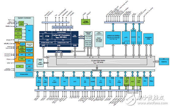
图1.SAM S70 144引脚框图
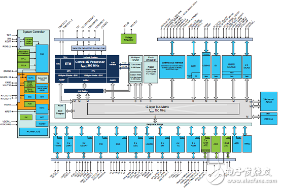
图2. SAM E70 144引脚框图
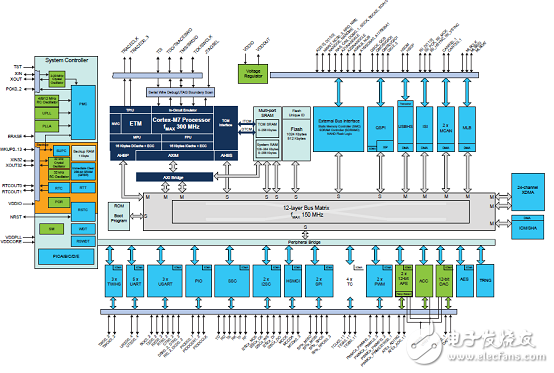
图3. SAM V70 144引脚框图
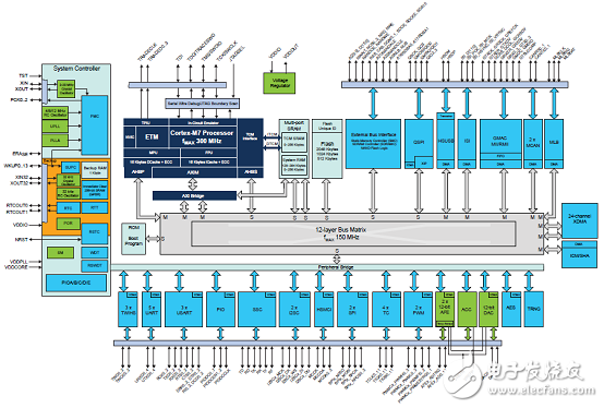
图4. SAM V71 144引脚框图
SAM E70 Xplained Ultra评估板DM320113
The SAM E70 Xplained Ultra Evaluation Kit is a hardware platform for evaluating the ATSAME70 and ATSAMS70 families of microcontrollers (MCU)。 Supported by both the Studio and MPLAB X integrated development platforms, the kit provide easy access to the features of the ATSAME70 and is a valuable assistant when integrating the device into a custom design.
The Xplained Ultra MCU series evaluation kits include an on-board Embedded Debugger, eliminating the need for external tools to program or debug the ATSAME70. The kit offers additional peripherals to extend the features of the board and ease the development of custom designs.
The Microchip PIC32 SAM E70 Xplained Ultra Development Kit (DM320113) provides a modulardevelopment system for Microchip’s line of 32-bit Cortex® microcontrollers.For a free Microchip demonstration code and additional information, visit the MPLAB Harmony™ webpage at:
The Atmel SAM E70 Xplained Ultra Dvelopment Kit is a hardware platform to evaluate the MicrochipATSAME70Q21. The kit offers a set of features that enables the ATSAME70Q21 users to start with theSAM E70 peripherals and understand how to integrate the device in their design.
The SAM E70 Xlpained Ultra kit contains the following items:
• One SAM E70 Xplained Ultra Development Kit
• One KSZ8061 Ethernet PHY
• One Graphics card set up for 565 (16-bit color) graphics
图5.SAM E70 Xplained Ultra评估板和PHY子板外形图
SAM E70 Xplained Ultra评估板DM320113主要特性:
• ATSAME70Q21 Microcontroller
• One Mechanical Reset Button
• One Mechanical User Push Button
• Two User LEDs
• 12.0 MHz Oscillator (DSC6003)
• 32.768 kHz Oscillator (DSC6083)
• 2-MB SDRAM
• 4-MB QSPI Flash (SST26VF032BA)
• Ethernet Interface with External IEEE 802.3az 10Base-T/100Base-TX Ethernet RMII PHY on aDaughter Board
• AT24MAC402 256KB EEPROM with EUI-48 Address
• ATA6561 CAN Transceiver
• Micro SD Card Connector with SDIO Support
• Camera Interface Connector
• Two Xplained Pro Extension Headers
• Graphics Card Interface
• CoreSight® 20 Connector for 4-bit ETM
• Arduino MEGA Shield Connector
• External Debugger Connector
• USB Interface, Device and Host Mode
• Embedded Debugger:
– Programming and debugging through USB interface
– Auto-ID for board identification in Atmel Studio and MPLAB® X
– One yellow status LED
– One green board power LED
– Symbolic debug of complex data types including scope information
– Data Gateway Interface: SPI, I2C, four GPIOs
– Virtual COM port (CDC)
• External Power Input (5-14V) or USB Power
• X32 Daughter Board Interface to Support Audio and Bluetooth®
• One mikroBus™ Interface
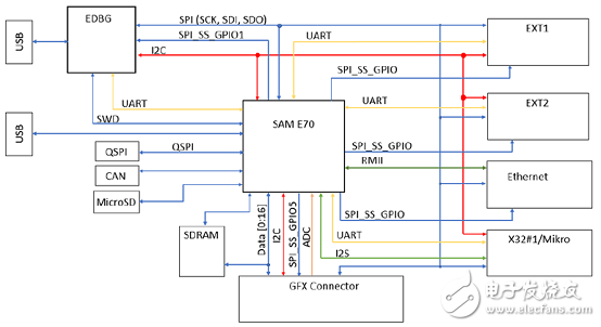
图6.SAM E70 Xplained Ultra评估板信号级框图
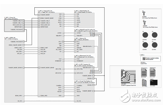
图7.SAM E70 Xplained Ultra评估板电路图(1)
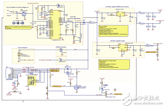
图8.SAM E70 Xplained Ultra评估板电路图(2)
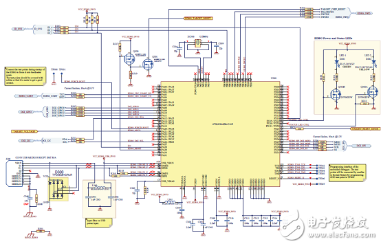
图9.SAM E70 Xplained Ultra评估板电路图(3)
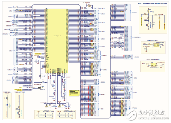
图10.SAM E70 Xplained Ultra评估板电路图(4)
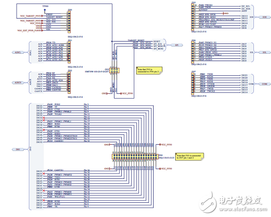
图11.SAM E70 Xplained Ultra评估板电路图(5)
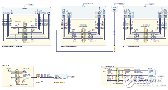
图12.SAM E70 Xplained Ultra评估板电路图(6)
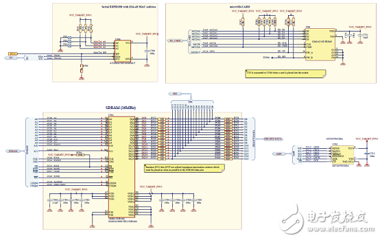
图13.SAM E70 Xplained Ultra评估板电路图(7)
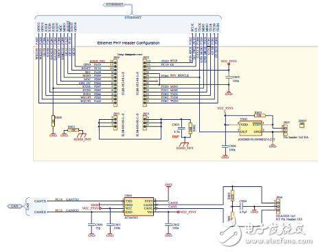
图14.SAM E70 Xplained Ultra评估板电路图(8)
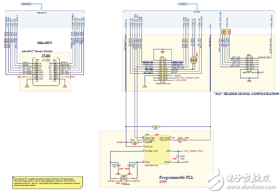
图15.SAM E70 Xplained Ultra评估板电路图(9)
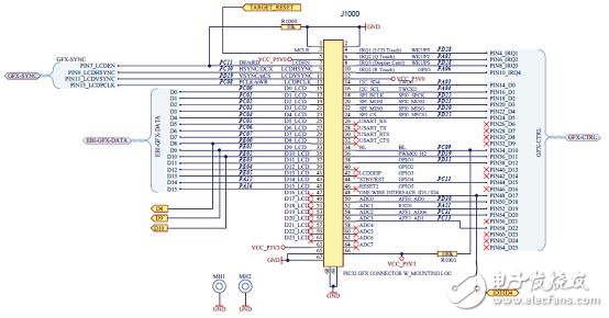
图16.SAM E70 Xplained Ultra评估板电路图(10)
SAM E70 Xplained Ultra评估板材料清单:
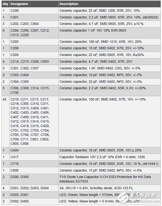
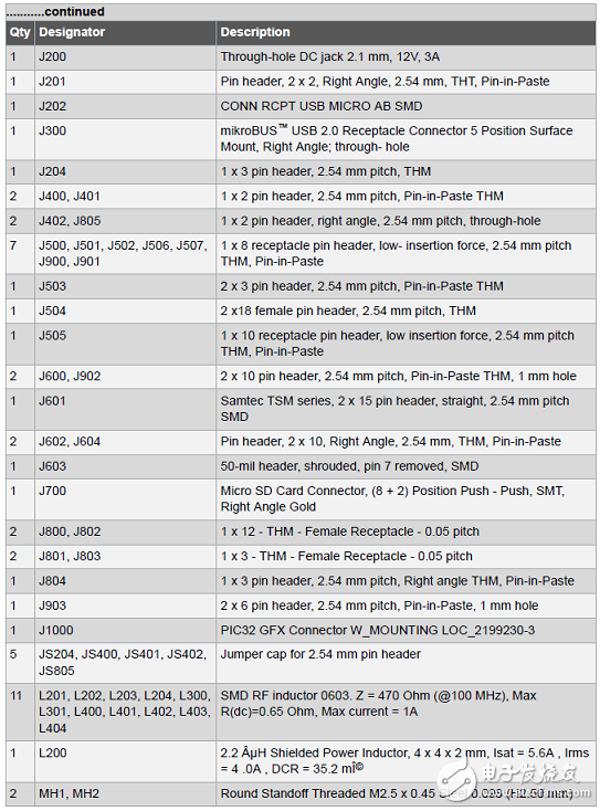
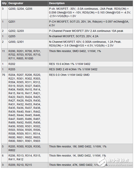
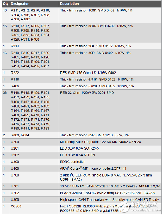
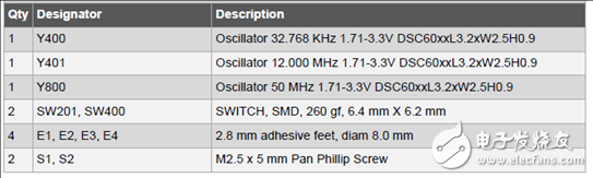
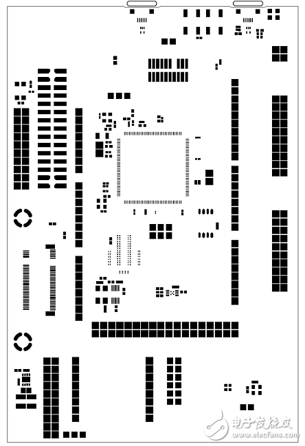
图17.SAM E70 Xplained Ultra评估板PCB设计图(1)
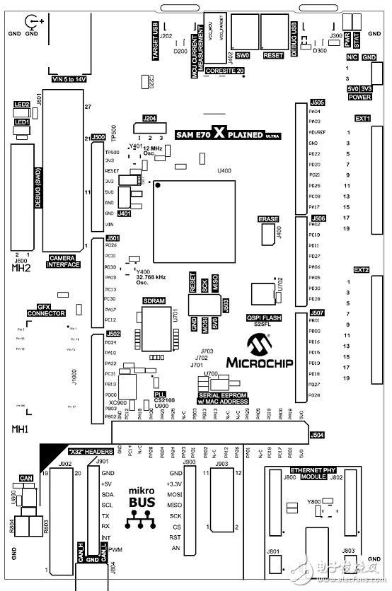
图18.SAM E70 Xplained Ultra评估板PCB设计图(2)
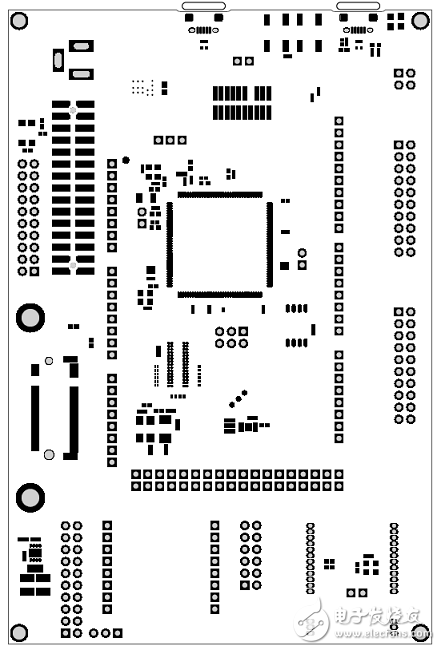
图17.SAM E70 Xplained Ultra评估板PCB设计图(1)
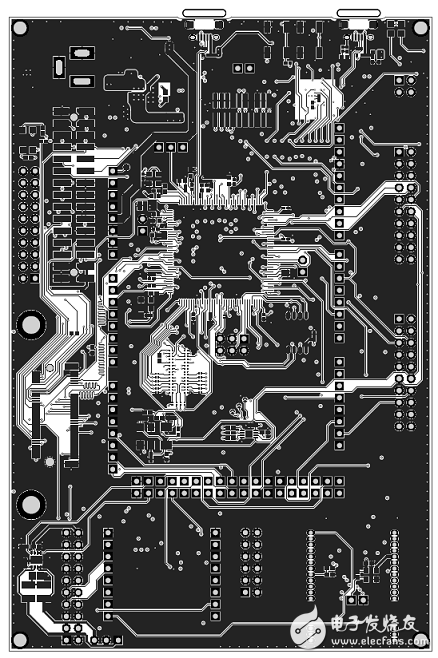
图18.SAM E70 Xplained Ultra评估板PCB设计图(2)
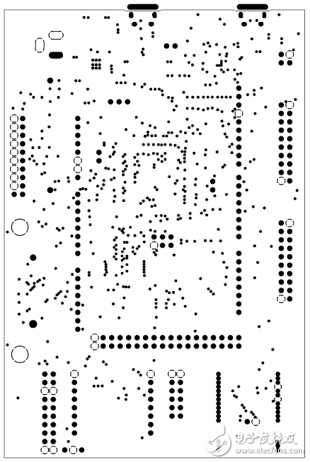
图19.SAM E70 Xplained Ultra评估板PCB设计图(3)
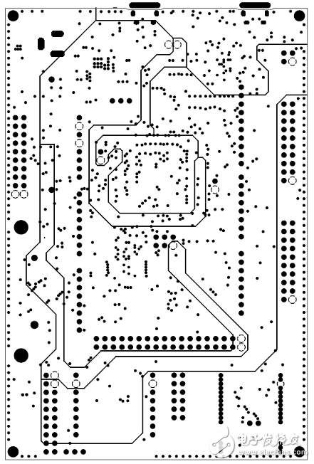
图20.SAM E70 Xplained Ultra评估板PCB设计图(4)
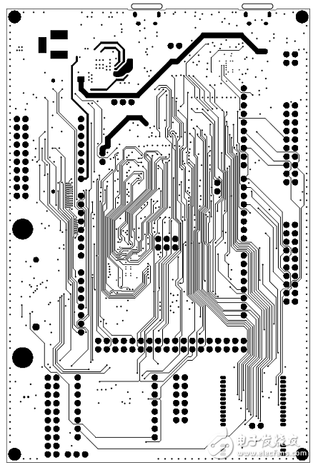
图21.SAM E70 Xplained Ultra评估板PCB设计图(5)
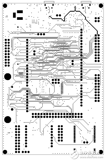
图22.SAM E70 Xplained Ultra评估板PCB设计图(6)
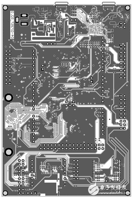
图23.SAM E70 Xplained Ultra评估板PCB设计图(7)
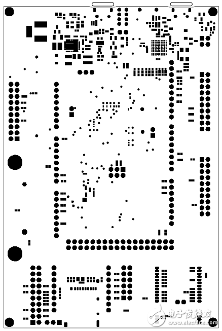
图24.SAM E70 Xplained Ultra评估板PCB设计图(8)
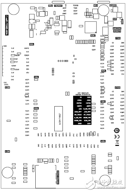
图25.SAM E70 Xplained Ultra评估板PCB设计图(9)
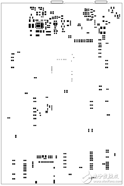
图26.SAM E70 Xplained Ultra评估板PCB设计图(10)
-
海尔电视电路图-21TA18-T2008-07-01 0
-
奥迪Q7电路图2009-10-08 0
-
[求助]熊猫21MF16电路图2010-03-02 0
-
创维8K21机芯电路图2010-12-17 0
-
检测电路图特性出现错误2014-05-29 0
-
jlink ob能不能仿真调试atsame70?2020-05-27 0
-
PIC32MX795F512主要特性及电路图是什么?2021-05-25 0
-
AK4678的主要特性是什么?其电路图是怎样的?2021-06-02 0
-
海尔21F2A、21F8D电路图2009-05-06 549
-
AD8452主要特性_框图以及应用电路2019-05-11 7272
-
CC1352P主要特性以及pcb电路图2019-04-05 6838
-
NCP51705主要特性_内部框图以及应用电路2019-05-11 4013
-
ISO224主要特性以及应用电路2019-04-05 10302
-
MAX40056主要特性以及应用电路2019-04-05 5390
-
MAX86150的优势特性以及典型应用电路图2019-04-05 5281
全部0条评论

快来发表一下你的评论吧 !
