

AP72200高效同步DC-DC升降压转换器解决方案
电子说
描述
Diodes公司的AP72200是大电流同步DC/DC升降压转换器,具有高效率,极好的瞬态响应和大DC输出精度.它采用四开关H桥配置,支持降压和升压工作,升/降压提供大于2A的输出电流.AP72200具有I2C兼容两线串行接口,包括双向串行数据线,SDA和串行时钟线,SCL.支持SCL时钟速率高达3.4MHz;此外,还具有UVLO,OTP和OCP保护电路.输入电压VIN从2.3V到5.5V,输出电压从2.6V-5.14V,连续输出电流2A,当VOUT=3.4V和 VIN>2.9V时效率高达97%.主要用在智能手机,平板电脑和其它手持设备.本文介绍了AP72200主要特性,功能框图,典型应用以及评估板AP72200-EVM主要特性,电路图,材料清单和PCB设计图.
The AP72200 is a high-current synchronous buck-boost converter providing high efficiency, excellent transient response, and high DC output accuracy. The targeted applications are smartphones, tablets, and other handheld devices. The AP72200 utilizes a four-switch H-bridge configuration to support buck and boost operation. The buck-boost provides at least 2A output current.
The current control scheme handles wide input/output voltage ratios and provides low external component count with outstanding performance in line/load transient response and seamless transition between buck and boost modes.
The AP72200 features I2C compatible, two-wire serial interface consisting of a bidirectional serial-data line, SDA, and a serial-clock line, SCL. It supports SCL clock rates up to 3.4MHz.
The AP72200 also features UVLO, OTP, and OCP to protect the circuit.
This IC is available in a small 2.125mm × 1.750mm, 20 balls WLCSP package.
AP72200主要特性:
• VIN 2.3V to 5.5V
• Output Voltage Range: 2.6V to 5.14V
• 2A Continuous Output Current for VOUT=3.4V and VIN>2.9V Efficiency Up to 97%
• 2.5MHz Switching Frequency
• I2C Interface
• Selectable MODE PFM/PWM
• Ultrasonic Operation Programmable through I2C
• Power Good Indicator with 5MΩ Internal Pull-Up
• Adjustable Overcurrent Limit
• Fully Protected for Overcurrent, Short Circuit, Reverse Current Protection, Overtemperature, and UVLO
• Totally Lead-Free & Fully RoHS Compliant (Notes 1 & 2)
• Halogen and Antimony Free. “Green” Device (Note 3)
AP72200应用:
• Smartphones
• Tablets
• Portable Consumer Devices
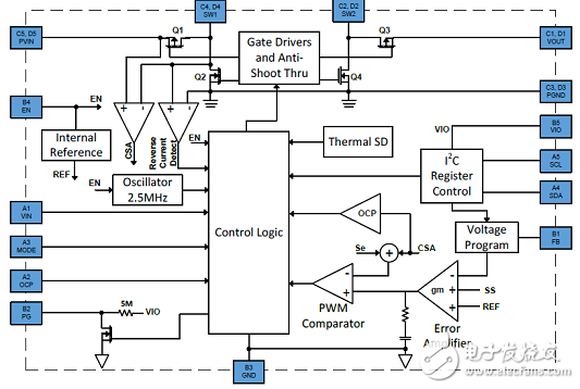
图1.AP72200框图
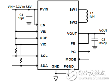
图2. AP72200典型应用
评估板AP72200-EVM
The AP72200 is a high current synchronous buck-boost converter providing high efficiency, excellent transient response and high DC output accuracy. The targeted applications are smartphones, tablets, and other handheld devices. The AP72200 utilizes a four switches H-bridge configuration to support buck and boost operation. The buck-boost provides at least 2A output current.
The current control scheme handles wide input/output voltage ratios and provides low external component count with outstanding performance in line/load transient response and seamless transition between buck and boost modes.
The AP72200 features I2C compatible, 2-wires serial interface consisting of a bidirectional serial-data line, SDA, and a serial-clock line, SCL. It supports SCL clock rates up to 3.4MHz.
The AP72200 also features UVLO, OTP, and OCP to protect the circuit.
This IC is available in a small 2.125x1.750mm, 20 balls WLCSP package
评估板AP72200-EVM主要特性:
VIN 2.3V to 5.5V
Output Voltage range: 2.6V to 5.14V
2A Continuous Output Current for VOUT=3.4V and VIN > 2.9V Efficiency Up to 97%
2.5MHz Switching Frequency
I2C Interface
Selectable MODE PFM/PWM
Ultrasonic Operation Programmable through I2C
Power Good Indicator with 5M Internal Pull-up
Adjustable Overcurrent Limit
Full Protected for Overcurrent,Short Circuit,Reverse Current Protection, Over Temperature, and UVLO
Totally Lead-Free & Fully RoHS Compliant
Halogen and Antimony Free. “Green” Device
应用:
Smartphones
Tablets
Portable Consumer Devices
图3.评估板AP72200-EVM外形图
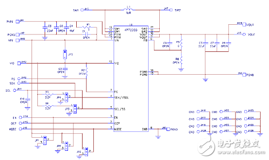
图4.评估板AP72200-EVM电路图
评估板AP72200-EVM材料清单:
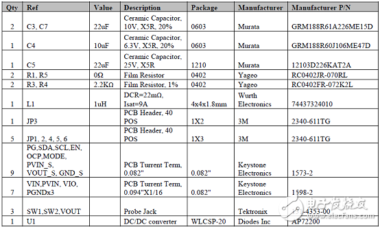
图5.评估板AP72200-EVM PCB设计图:顶层
图6.评估板AP72200-EVM PCB设计图:底
-
DC-DC转换器是什么及其参数2009-11-14 0
-
DC-DC转换器2010-03-09 0
-
AP3429A应用电路2A降压DC-DC转换器2019-03-07 0
-
AP3419应用电路2A降压DC-DC转换器2019-03-08 0
-
AP3502 340kHz,2A同步DC-DC降压转换器的典型应用2019-03-14 0
-
电子书:DC-DC 转换器的应用与设计方案2019-03-14 0
-
ADP2139CB-1.8EVALZ,是高效率,低静态电流,同步降压DC-DC转换器2019-07-18 0
-
高效率的Ap1603升压型DC-DC转换器的应用2020-06-18 0
-
DC-DC电源转换器/基准电压源介绍2021-10-28 0
-
一款非常高效的DC-DC降压转换器2022-07-07 0
-
DC-DC降压-升压转换器12V/4A的资料分享2022-09-05 0
-
高效的DC-DC降压转换器2022-07-08 730
-
AP3418高效率同步DC-DC降压转换器应用笔记2023-07-25 297
-
TDK 加强型300W DC-DC升降压转换器2024-02-06 273
全部0条评论

快来发表一下你的评论吧 !
