

PSoC 6高性能超低功耗IoT应用方案
电子说
描述
cypress公司的PSoC® 6 MCU系列产品是用于物联网(IoT)的高性能超低功耗和安全MCU平台,组合了双核微控制器和低功耗闪存技术,数字可编逻辑,高性能模数转换,标准通信和定时外设,并提供BLE 5.0兼容的无线连接.其32位双核CPU子系统包括150-MHz Arm® Cortex®-M4F CPU和100-MHz Cortex-M0+ CPU,用户可选择的核逻辑工作电压1.1V或0.9V,集成了双CPU核的8KB指令缓存,1.1V核工作时Cortex-M4为40 μA/MHz,Cortex-M0+为20 μA/MHz,而0.9V核工作时Cortex-M4为22μA/MHz,Cortex-M0+为15μA/MHz;两个DMA控制器每个有16路,低功耗蓝牙BT5.0子系统具有50W天线驱动的2.4GHz RF收发器,数字PHY,链接层引擎支持主从模式和同时四个连接,可编输出功率高达4dBm,RX灵敏度-95dBm,RSSI为4dB分辨率,支持2Mbps LE数据速率,低功耗1.7V-3.6V工作.本文介绍了PSoC® 6 MCU系列主要特性,框图,时钟图和电源连接图以及原型板PSoC 6 Wi-Fi BT主要特性,框图和电路图.
PSoC® 6 MCU is a high-performance, ultra-low-power and secure MCU platform, purpose-built for IoT applications. The PSoC 63with BLE product family, based on the PSoC 6 MCU platform, is a combination of a dual core microcontroller with low-power flashtechnology, digital programmable logic, high-performance analog-to-digital and standard communication and timing peripherals.ThePSoC 63 family provides wireless connectivity with BLE 5.0 compliance.
PSoC® 6 MCU系列主要特性:
32-bit Dual-Core CPU Subsystem
■ 150-MHz Arm® Cortex®-M4F CPU with single-cycle multiply(Floating Point and Memory Protection Unit)
■ 100-MHz Cortex-M0+ CPU with single-cycle multiply and MPU
■ User-selectable core logic operation at either 1.1 V or 0.9 V
■ 8-KB Instruction Caches for both CPU cores
■ Active CPU current slope with 1.1-V core operation
❐Cortex-M4: 40 μA/MHz
❐Cortex-M0+: 20 μA/MHz
■ Active CPU current slope with 0.9-V core operation
❐Cortex-M4: 22 μA/MHz
❐Cortex-M0+: 15 μA/MHz
■ Two DMA controllers with 16 channels each
Flash Memory Subsystem
■ 1-MB Application Flash, 32-KB emulated EEPROM area, and32-KB Supervisory Flash
■ 288-KB SRAM with power and data retention control
■ One-Time-Programmable (OTP) 1-Kb eFuse memory forvalidation and security
Bluetooth Low Energy (Bluetooth Smart) BT 5.0Subsystem
■ 2.4-GHz RF transceiver with 50-W antenna drive
■ Digital PHY
■ Link Layer engine supporting master and slave modes
■ Programmable output power: up to 4 dBm
■ RX sensitivity: –95 dBm
■ RSSI: 4-dB resolution
■ 5.7 mA TX (0 dBm) and 6.7 mA RX (2 Mbps) current with 3.3-Vbattery and internal SIMO Buck converter
■ Link Layer engine supports four connections simultaneously
■ Supports 2 Mbps LE data rate
Low-Power 1.7-V to 3.6-V Operation
■ Six power modes for fine-grained power management
■ Deep Sleep mode current of 7 μA with 64-KB SRAM retention
■ On-chip Single-In Multiple Out (SIMO) DC-DC Buck converter,<1 μA quiescent current
■ Backup domain with 64 bytes of memory and Real-Time Clock
Flexible Clocking Options
■ On-chip crystal oscillators (4 to 35 MHz, and 32 kHz)
■ Phase-locked Loop (PLL) for multiplying clock frequencies
■ 8 MHz Internal Main Oscillator (IMO) with ±2% accuracy
■ Ultra-low-power 32-kHz Internal Low-speed Oscillator (ILO)
■ frequency Locked Loop (FLL) for multiplying IMO frequency
QSPI Interface (QSPI)/Serial Memory Interface (SMIF)
■ Execute-In-Place (XIP) from external Quad SPI Flash
■ On-the-fly encryption and decryption
■ 4-KB cache for greater XIP performance with lower power
■ Supports single, dual, quad, dual-quad, and octal interfaces w/throughput up to 640 Mbps
Serial Communication
■ Nine run-time configurable serial communication blocks(SCBs)
❐Eight SCBs: configurable as SPI, I2C, or UARTs
❐One Deep Sleep SCB: configurable as SPI or I2C
■ USB Full-Speed Dual-role Host and Device interface
Audio Subsystem
■ Two PDM channels and one I2S channel with TDM mode
Programmable Analog
■ 12-bit 1-Msps SAR ADC with differential and single-endedmodes and 16-channel sequencer with result averaging
■ Two low-power comparators available in Deep Sleep andHibernate modes
■ Built-in temp sensor connected to ADC
■ One 12-bit voltage mode DAC with < 5-μs settling time
■ Twoopamps with low-power operation modes
Up to 78 Programmable GPIOs
■ Two Smart I/O ports (16 I/Os) enable Boolean operations onGPIO pins; available during Deep Sleep
■ Programmable drive modes, strengths, and slew rates
■ Six overvoltage-tolerant (OVT) pins
Capacitive Sensing
■ Cypress CapSense Sigma-Delta (CSD) provides best-in-classSNR, liquid tolerance, and proximity sensing
■ Enables dynamic usage of both self and mutual sensing
■ Automatic hardware tuning (SmartSense™)
Security Built into Platform Architecture
■ ROM-based root of trust via uninterruptible Secure Boot
■ Step-wise authentication of execution images
■ Secure execution of code in execute-only mode for protectedroutines
■ All Debug and Test ingress paths can be disabled
■ Up to eight Protection Contexts
Cryptography Accelerators
■ Hardware acceleration for symmetric and asymmetriccryptographic methods and hash functions
■ True Random Number Generator (TRNG) function
Programmable Digital
■ 12 programmable logic blocks, each with 8 Macrocells and an8-bit data path (called universal digital blocks or UDBs)
■ Usable as drag-and-drop Boolean primitives (gates, registers),or as Verilog programmable blocks
■ Cypress-provided peripheral component library using UDBs toimplement functions such as Communication peripherals (forexample, LIN, UART, SPI, I2C, S/PDIF and other protocols),Waveform Generators, Pseudo-Random Sequence (PRS)generation, and many other functions.)
Energy Profiler
■ Block that provides history of time spent in different powermodes
■ Allows software energy profiling to observe and optimizeenergy consumption
Packages
■ 116-BGA and 104-MCSP packages with PSoC 6 and BLERadio
■ 104-MCSP package with BLE Radio and USB
■ 124-BGA package in the process of qualification
■ 68-QFN package
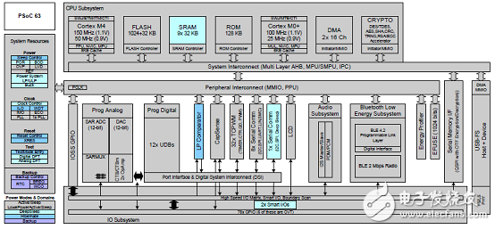
图1.PSoC® 6 MCU系列框图
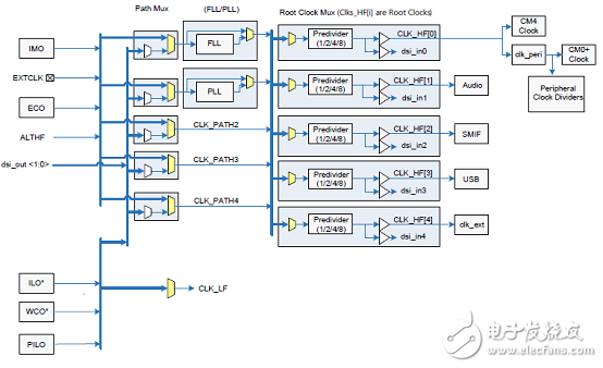
图2.PSoC® 6 MCU系列时钟框图
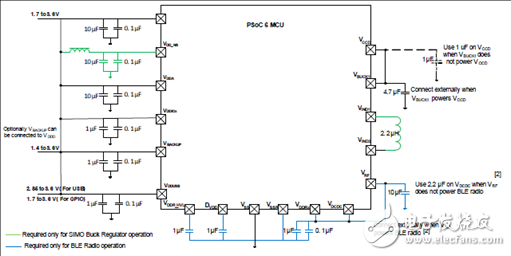
图3.PSoC® 6 MCU系列电源连接图
评估板CY8CPROTO-062-4343W PSoC 6 Wi-Fi BT
Thank you for your interest in the CY8CPROTO-062-4343W PSoC 6 Wi-Fi BT Prototyping Kit. ThePSoC 6 Wi-Fi BT Prototyping Kit enables you to evaluate and develop your applications using thePSoC 6 MCU and CYW4343W WICED Wi-Fi/BT combo device.
PSoC 6 MCU is Cypress’latest, ultra-low-power PSoC specifically designed for wearables and IoTproducts. PSoC 6 MCU is a true programmable embedded system-on-chip, integrating a 150-MHzArm® Cortex®-M4 as the primary application processor, a 100-MHz Arm Cortex®-M0+ that supportslow-power operations, up to 2 MB Flash and 1 MB SRAM, Secure Digital Host Controller (SDHC)supporting SD/SDIO/eMMC interfaces, CapSense® touch-sensing, and programmable analog anddigital peripherals that allow higher flexibility, in-field tuning of the design, and faster time-to-market.
You can use ModusToolbox™ to develop and debug your PSoC 6 MCU and CYW4343W
applications. ModusToolbox software is a set of tools that enable you to integrate Cypress devicesinto your existing development methodology. One of the tools is a multi-platform, Eclipse-basedIntegrated Development Environment (IDE) that supports configuration and applicationdevelopment, called ModusToolbox IDE.
评估板CY8CPROTO-062-4343W PSoC 6 Wi-Fi BT包括:
■ PSoC 6 Wi-Fi BT Prototyping Board
■ USB Type-A to Micro-B cable
■ Quick Start Guide (printed on the kit package)
原型板PSoC 6 Wi-Fi BT主要特性:
■ CY8CMOD-062-4343W PSoC 6 MCU with CYW4343W Wi-Fi BT module that contains
❐PSoC 6 MCU with SDHC
❐Murata Type 1DX ultra-small 2.4-GHz WLAN and Bluetooth functionality module based onCYW4343W
■ microSD card slot
■ 512-Mbit external Quad SPI NOR Flash that provides a fast, expandable memory for data andcode
■ A thermistor to measure ambient temperature and two PDM microphones for voice input
■ KitProg3 onboard SWD programmer/debugger with USB-UART and USB-I2C bridge functionality
■ CapSense touch-sensing slider (5 elements) and two CapSense buttons, all of which are capableof both self- capacitance (CSD) and mutual-capacitance (CSX) operation
■ A Micro-B connector for USB device interface and a separate Micro-B connector for programming/debug using the KitProg3
■ Expansion headers that are compatible with Digilent® Pmod™ modules
■ 1.8 V and 3.3 V operation of PSoC 6 MCU is supported
■ One user LED, a user button, and a reset button for PSoC 6 MCU
■ One Mode selection button and one Mode LED for KitProg3
图4.原型板PSoC 6 Wi-Fi BT外形图
原型板PSoC 6 Wi-Fi BT对应的数字内容:
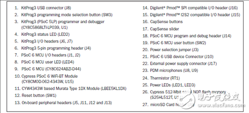
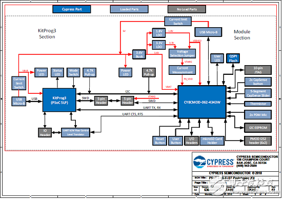
图5.原型板PSoC 6 Wi-Fi BT电路图(1)
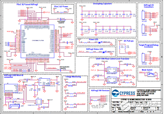
图6.原型板PSoC 6 Wi-Fi BT电路图(2)
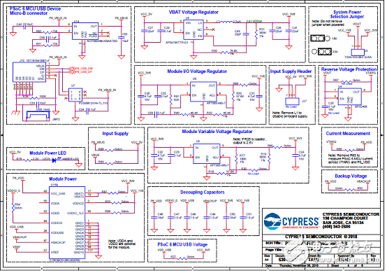
图7.原型板PSoC 6 Wi-Fi BT电路图(3)
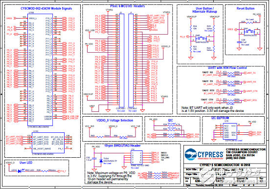
图8.原型板PSoC 6 Wi-Fi BT电路图(4)
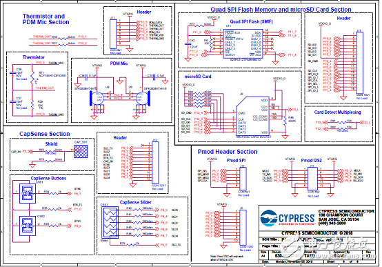
图9.原型板PSoC 6 Wi-Fi BT电路图(5)
图10.原型板PSoC 6 Wi-Fi BT电路图(6)
- 相关推荐
- IOT
-
Cypress PSoC蓝牙低功耗开发设计攻略2015-05-08 0
-
【FireBLE申请】超低功耗智能手环研发2015-07-08 0
-
SKYLAB三款超低功耗gps模块应用2017-06-20 0
-
小尺寸、超低功耗的智能穿戴定位解决方案2017-09-28 0
-
超低功耗FPGA解决方案助力机器学习2018-05-23 0
-
赛普拉斯的PSoC®6 IOT微控制器的功能2018-10-31 0
-
安森美半导体的IoT应用怎么样?2019-08-09 0
-
超低功耗Wi-Fi技术2020-05-24 0
-
赛普拉斯IoT-AdvantEdge解决方案!2020-09-01 0
-
无线互联是IoT的应用有哪些?2020-11-30 0
-
STM8超低功耗系列2021-08-23 0
-
PSOC6核心板的资料分享2022-08-15 0
-
超低功耗MCU在物联网方案中的应用2023-06-13 0
-
低功耗ADC实现高性能明智设计2012-03-13 751
-
藍牙4.0 超低功耗藍牙空中鼠標解決方案2018-10-04 281
全部0条评论

快来发表一下你的评论吧 !
