

ADF5610宽带微波频率合成器集成压控振荡器解决方案
电子说
描述
ADI公司的ADF5610是微波宽带压控振荡器(VCO),工作频率从3700MHz到14600MHz,单个射频(RF)输出.ADF5610和外接回路滤波器和外接基准源一起,能实现分数N或整数N锁相环(PLL)频率合成器.带差分频率输出的分频器工作在57 MHz 到14600 MHz,而PLL电路的模拟和数字电源从3.1V到3.5V,而VCO的工作在4.75V-5,25V,电荷泵的电源可扩展到3.6V.ADF5610还集成了基频从3650 MHz到7300 MHz的VCO,其差分输出允许倍频VCO频率能进行1, 2, 4, 8, 16, 32, 64或128分频,使得用户可获得低至57MHz RF输出频率.集成的鉴相器(PD)和delta-sigma (Δ-Σ)调制器,工作高达100MHz,其杂散电平为-100dBc.而相位噪音电平从7.3GHz的−115 dBc/Hz到14.6GHz的−109 dBc/Hz. RFOUT功率5dbm,可编程输出功率电平,典型功耗815mW.主要用在军用和国防,测试设备,时钟发生器,无线基础设备,卫星和甚小孔径终端(VSAT),微波无线电.本文介绍了ADF5610主要特性,功能框图,PLL和VCO子系统框图,以及评估板EV-ADF5610SD1Z主要特性,电路图,材料清单和PCB设计图.
The ADF5610 allows implementation of fractional-N or Integer N phase-locked loop (PLL) frequency synthesizers when used with an external loop filter and an external reference source. The wideband microwave voltage controlled oscillator (VCO) design permits frequency operation from 7300 MHz to 14600 MHz at a single radio frequency (RF) output. A series of frequency dividers with a differential frequency output allows operation from 57 MHz to 14600 MHz.Analog and digital power supplies for the PLL circuitry range from 3.1 V to 3.5 V, and the VCO supplies are between 4.75 V and 5.25 V. The charge pump supply voltage can be extended up to 3.6 V for improved frequency band overlap and extended upper frequency range.
The ADF5610 has an integrated VCO with a fundamental frequency of 3650 MHz to 7300 MHz. These frequencies are internally doubled and routed to the RFOUT pin. An additional differential output allows the doubled VCO frequency to be divided by 1, 2, 4, 8, 16, 32, 64, or 128, allowing the user to generate RF output frequencies as low as 57 MHz. A simple 3-wire serial port interface (SPI) provides control of all on-chip registers. To conserve power, this divider block can be disabled when not needed through the SPI interface. Likewise, the output power for both the single-ended output and the differential output are programmable via the VCO register settings. The ADF5610 also contains various power-down modes for the VCO circuitry and PLL circuitry.
The integrated phase detector (PD) and delta-sigma (Δ-Σ) modulator, capable of operating at up to 100 MHz, permit wide loop bandwidths and fast frequency tuning with a typical spurious level of −100 dBc.
With phase noise levels from −115 dBc/Hz at 7.3 GHz to −109 dBc/Hz at 14.6 GHz, the ADF5610 is equipped to minimize blocker effects, and to improve receiver sensitivity and transmitter spectral purity. The low phase noise floor eliminates any contribution to modulator and mixer noise floor in transmitter applications.
The ADF5610 is a PLL with integrated VCO. The device features an innovative programmable performance technology that enables the ADF5610 to tailor current consumption and corresponding noise performance to individual applications by selecting either a low current consumption mode or a high performance mode for improved phase noise performance.
Additional features of the ADF5610 include approximately 3 dB of RFOUT gain control in 1.5 dB steps and 5 dB of control on the differential port in approximately 2.5 dB steps. Finally, the Δ-Σ modulator with exact frequency mode enables users to generate output frequencies with 0 Hz frequency error.
ADF5610主要特性:
RF output frequency range: 57 MHz to 14,600 MHz
RFOUT: 7300 MHz to 14,600 MHz
PDIV/NDIV: 57 MHz to 14,600 MHz
Fractional-N synthesizer and Integer N synthesizer modes
24-bit fractional modulus
Exact frequency mode for 0 Hz frequency error
Typical PFD spurious: <−105 dBc
Integrated rms jitter: <40 fs
Normalized inband phase noise floor FOM
High current mode: −232 dBc/Hz (integer) and −229 dBc/Hz (fractional)
Normal mode: −229 dBc/Hz (integer) and −226 dBc/Hz (fractional)
Maintains frequency lock over −40℃ to +85℃ (lock and leave)
Low phase noise VCO
−115 dBc/Hz typical at 100 kHz (7.3 GHz)
−114 dBc/Hz typical at 100 kHz (10 GHz)
−109 dBc/Hz typical at 100 kHz (14.6 GHz)
RFOUT power: 5 dBm
Programmable divide by 1, 2, 4, 8, 16, 32, 64, or 128 output
Programmable output power level
Typical power dissipation: 815 mW
Programmable low current and power dissipation: <700 mW
Fast frequency hopping (autocalibration enabled): <40 μs
48-terminal, 7 mm×7 mm LGA package: 49 mm2
ADF5610应用:
Military and defense
Test equipment
Clock generation
Wireless infrastructure
Satellite and very small aperture terminal (VSAT)
Microwave radio
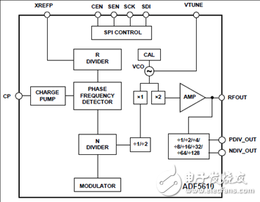
图1.ADF5610功能框图
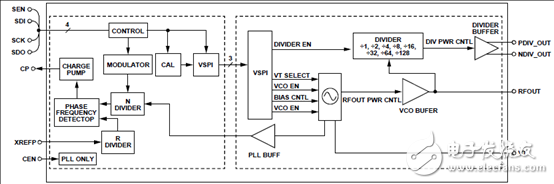
图2.PLL和VCO子系统框图
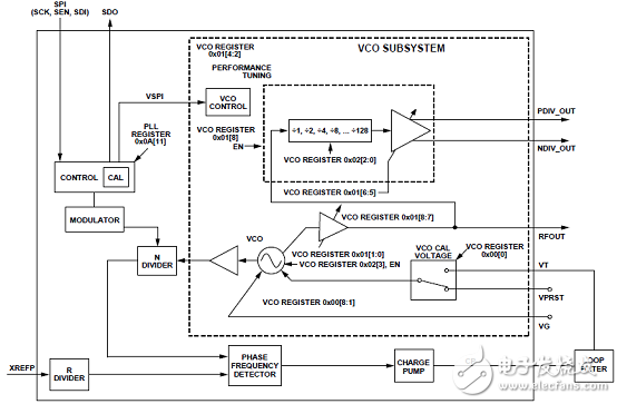
图3.PLL和VCO子系统详细框图
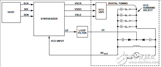
图4.简化调谐VCO图
评估板EV-ADF5610SD1Z
The EV-ADF5610SD1Z evaluates the performance of the ADF5610 frequency synthesizer with integrated VCO for phase-locked loops (PLLs). A photograph of the evaluation board is shown in Figure 1. The evaluation board contains the ADF5610 synthesizer with integrated voltage controlled oscillator (VCO), a low noise, single-ended, 50 MHz voltage controlled crystal oscillator (VCXO) reference, the HMC1031 Integer N PLL, a switch, a jumper, a loop filter, a USB interface, and subminiature Version A (SMA) connectors.
For easy programming of the synthesizer, download the Windows®-based software from the ADF5610 page at ftp://ADF5610_ftp:ZagrJ6Fx@ftp.analog.com. The file transfer program (FTP) user name and password are printed on the label inside the lid of the evaluation board box. The user manual and evaluation printed circuit board (PCB) schematic can also be found on the FTP site.
The EV-ADF5610SD1Z evaluation board requires a SDP-S controller board (see Figure 3), which is not included with the kit. The SDP-S allows software programming of the ADF5610 device through a USB interface.
Full specifications for the ADF5610 wideband microwave synthesizer are available in the ADF5610 data sheet, which must be consulted in conjunction with this user guide when working with the evaluation board.
评估板EV-ADF5610SD1Z主要特性:
Self contained board, including ADF5610 frequency synthesizer with integrated VCO, single-ended, 50 MHz VCXO, PLL jitter clean up circuit, loop filter (4 kHz), USB interface, and voltage regulators
Windows-based software allows control of synthesizer functions from a PC
Externally powered by a single 6 V supply
图6.评估板EV-ADF5610SD1Z外形图
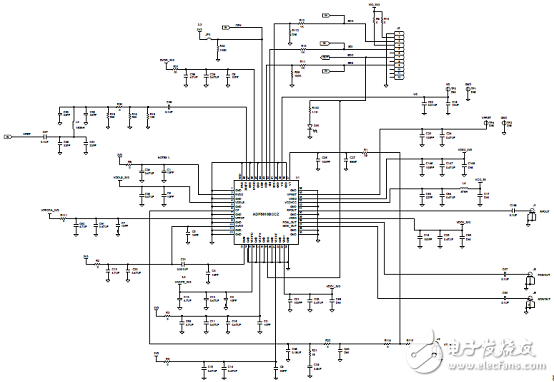
图7.评估板EV-ADF5610SD1Z电路图(1)
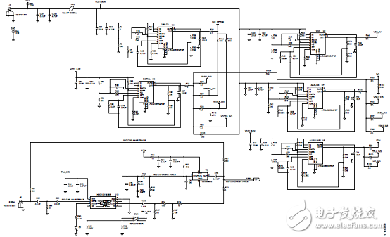
图8.评估板EV-ADF5610SD1Z电路图(2)
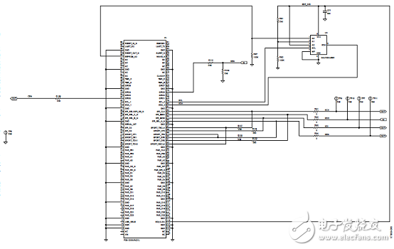
图9.评估板EV-ADF5610SD1Z电路图(3)
评估板EV-ADF5610SD1Z材料清单:
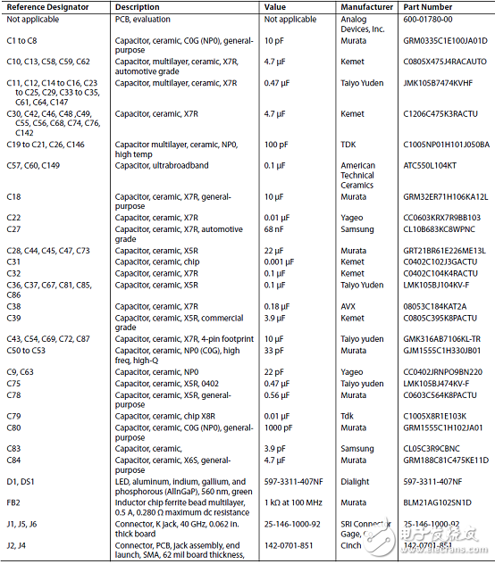
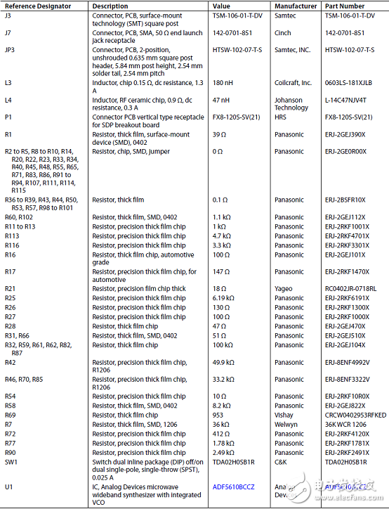
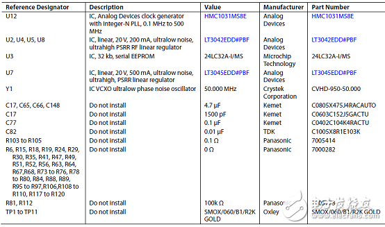
图10.评估板EV-ADF5610SD1Z PCB设计图(1):丝印和金属1,顶层
图11.评估板EV-ADF5610SD1Z PCB设计图(2):金属2,地层
图12.评估板EV-ADF5610SD1Z PCB设计图(3):金属3,RF和DC
图13.评估板EV-ADF5610SD1Z PCB设计图(4):金属4,背面
-
集成压控振荡器数据表的微波宽带合成器ADF53562021-05-20 461
-
集成压控振荡器的宽带锁相环真的能取代分立式解决方案吗?2019-07-31 0
-
贸泽电子正式开售ADF5610宽带频率合成器2020-12-18 0
-
贸泽开售相位噪声超低的Analog Devices ADF5610宽带频率合成器2019-12-09 1566
-
集成压控振荡器数据表的微波宽带合成器ADF4355-22021-04-14 409
-
集成压控振荡器数据表的微波宽带合成器ADF53552021-04-14 459
-
UG-1409:评估集成压控振荡器的ADF5610宽带微波合成器2021-04-20 387
-
集成压控振荡器数据表的微波宽带合成器ADF43722021-04-22 557
-
集成压控振荡器数据表的微波宽带合成器ADF43552021-04-23 518
-
集成压控振荡器数据表的微波宽带合成器ADF4355-32021-04-28 419
-
UG-805:集成压控振荡器的ADF4355微波宽带合成器评估2021-05-09 425
-
ADF4356:集成压控振荡器数据表的6.8 GHz宽带合成器2021-05-11 593
-
UG-1548:评估集成压控振荡器的ADF4372微波宽带合成器2021-05-12 389
-
UG-1474:评估集成压控振荡器的ADF4371微波宽带合成器2021-05-16 395
-
UG-1062:评估集成压控振荡器的ADF4356微波宽带合成器2021-05-22 404
全部0条评论

快来发表一下你的评论吧 !
