

双输出多相电流模式同步控制方案
电子说
描述
ADI公司的LTCR7852/LTC7852-1是6相双输出电流模式同步降压开关稳压器控制器,和外接功率器件如DrMOS,功率区块或分立N沟MOSFET和相关的栅极驱动器。它可以进行1-,2-,3-,4-,5-和6相配置。采用两个IC并联可配置成8-,10和12相,以得到高达400A电流。亚毫欧姆DCR检测或DrMOS电流检测改善了效率,总输出电压精度±0.5%,具有灵活的相位配置和双输出电流监视,双差分遥测放大器,可编频率范围从250kHz到1.2MHz,VIN范围不受IC所限,VCC范围4.5V-5.5V,VOUT范围从0.5V到2.0V.主要用在计算机系统,通信和数据系统以及DC电源分布系统。本文介绍了LTC7852-1主要特性,功能框图,典型应用电路和多种应用电路,以及演示板DC2631A主要特性,框图,测试建立图,以及电路图,材料清单和PCB设计图。
The LTCR7852/LTC7852-1 is a six-phase, dual outputcurrent mode synchronous step-down switching regulatorcontroller that works in conjunction with externalpower train devices such as DrMOS, power blocks ordiscrete N-channel MOSFETs and associated gate drivers.
Its flexible design enables 1-, 2-, 3-, 4-, 5-, and 6-phaseconfigurations. The LTC7852 offers a unique feature thatenhances the signal-to-noise ratio of the current sensesignal, allowing the use of inductors with very low DCwinding resistances for maximum efficiency. The controllerachieves a minimum on-time of just 40ns, permitting theuse of high switching frequency at high step-down ratios.
8-, 10- or 12 phases with two ICs can be paralleled forvery high current requirements up to 400A.The remote sense differential amplifiers and a precisereference provide accurate output voltages between 0.5Vand 2.0V. The input voltage is not limited by the controller. Hiccup mode protection from output shorts or overcurrentminimizes the thermal dissipation.
The LTC7852-1 is designed specifically for DrMOS withan internal current sense signal.
LTC7852-1主要特性:
Sub-Milliohm DCR Sensing or DrMOS with CurrentSense Improves Efficiency
Operates with Power Blocks, DrMOS or ExternalGate Drivers and MOSFETs
±0.5% Total Output Voltage Accuracy
Flexible Phase Configuration
Dual Output Current Monitoring
tON(MIN) = 40ns, Capable of Very Low Duty Cycles atHigh Frequency
Dual Differential Remote Sensing Amplifiers
Programmable Frequency Range of 250kHz to 1.2MHz
VIN Range Is Not Limited by IC
VCC Range: 4.5V to 5.5V
VOUT Range: 0.5V to 2.0V
48 Lead (5mm × 6mm) GQFN for LTC7852
36 Lead (4mm × 5mm) QFN for LTC7852-1
LTC7852-1应用:
Computer Systems
Telecom and Datacom Systems
DC Power Distribution Systems
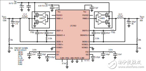
图1.LTC7852-1典型应用电路
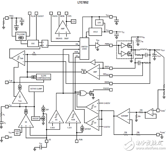
图2.LTC7852-1功能框图
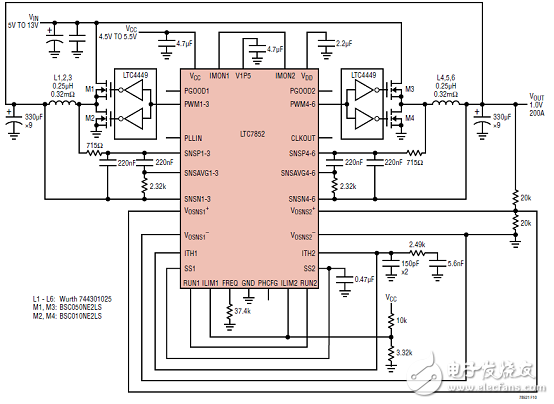
图3.带分立驱动器和MOSFET的LTC7852单输出6相1V/200A转换器电路
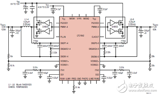
图4.带DRMOS的LTC7852双输出4相0.9V/120A和2相1.2V/60A转换器电路
演示板DC2631A
Demonstration circuit 2631A features the LTC®7852 in two high output current, high efficiency step down converters each with its own assembly type. The converter for the -A assembly provides two 3-phase outputs of 1.0V/100A and 1.5V/100A. The -B assembly provides a single 6-phase 1.0V/200A output. Block diagrams are shown in Figure 3. Both converters operate over a 7V to 14V input voltage range at a switching frequency of 400kHz.
The power stage for each phase consists of a 5mm × 5mm DrMOS and 11.3mm × 11.0mm 0.25μH ferrite inductor with a DCR of 0.32mΩ typical. The LTC7852 employs a peak current mode architecture which allows accurate DCR sensing and sharing with sub-mOhm DCR inductors. The LTC7852 provides a three-state compatible PWM output for each DrMOS.
演示板DC2631A主要特性:
Additional features of the DC2631A include:
lDifferential sensing for the output voltages of VOUT1 and VOUT2
lIMON pins to monitor the inductor current of each rail.
l Optional resistors and jumpers to change the phase arrangement for VOUT1 and VOUT2:
q VOUT1: 4ph, VOUT2: 2ph
q VOUT1: 5ph, VOUT2: 1ph
q Note, the default arrangement is: VOUT1: 3ph, VOUT2: 3ph
l Optional resistors and jumpers to parallel VOUT1 and VOUT2.
l RUN, PGOOD, PLLIN and CLKOUT pins
The LTC7852 data sheet provides a complete description of the IC operation and application information. The data sheet must be read in conjunction with the quick start guide.
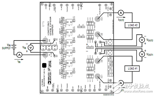
图5.演示板DC2631A-A测试建立图
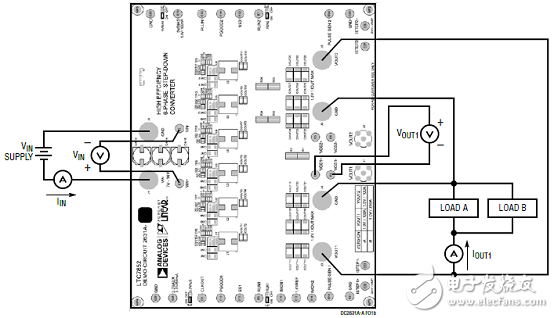
图6.演示板DC2631A-B测试建立图
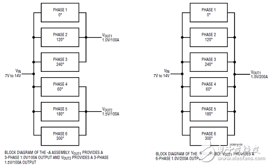
图7.演示板DC2631A-A/DC2631B-B框图
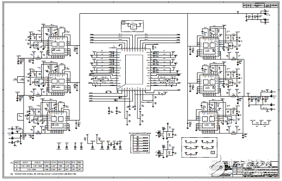
图8.演示板DC2631A电路图(1)
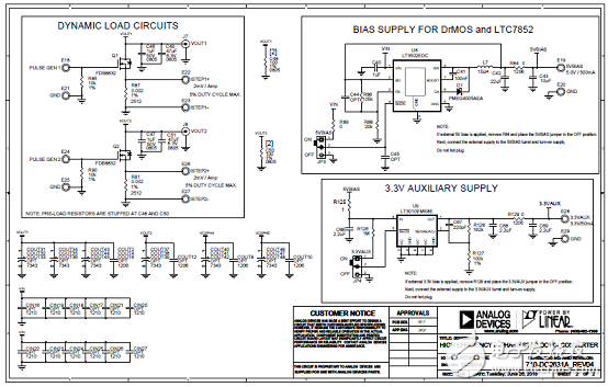
图9.演示板DC2631A电路图(2)
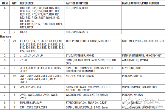
演示板DC2631A-A材料清单:
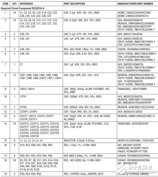
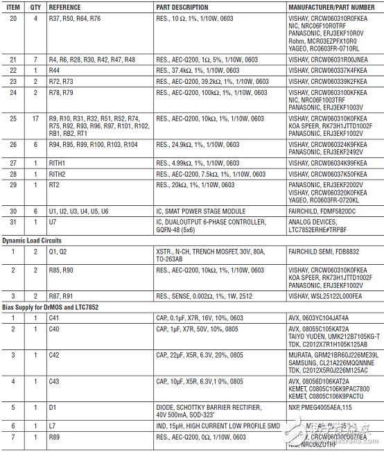
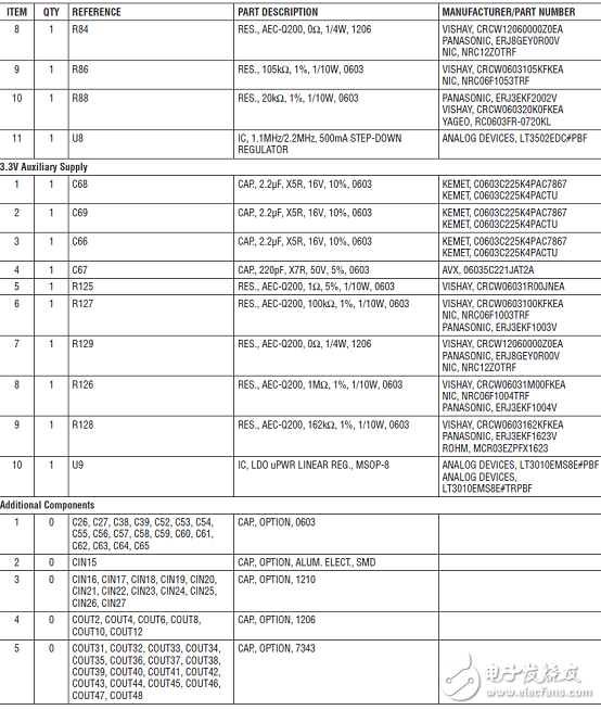
演示板DC2631A-B材料清单:
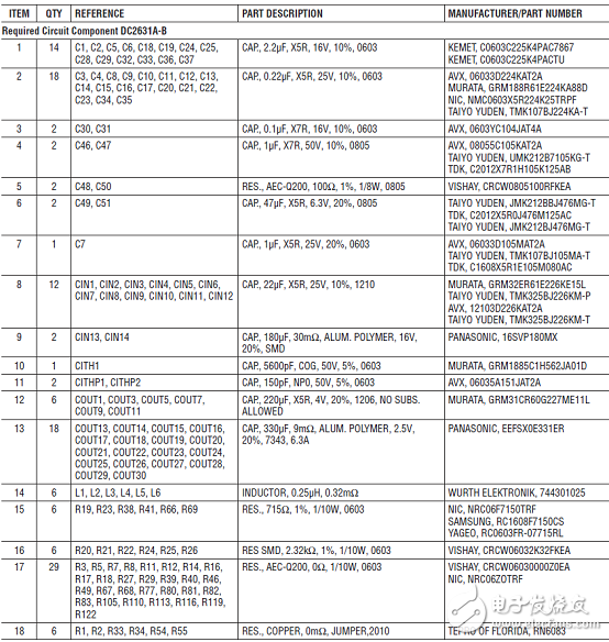
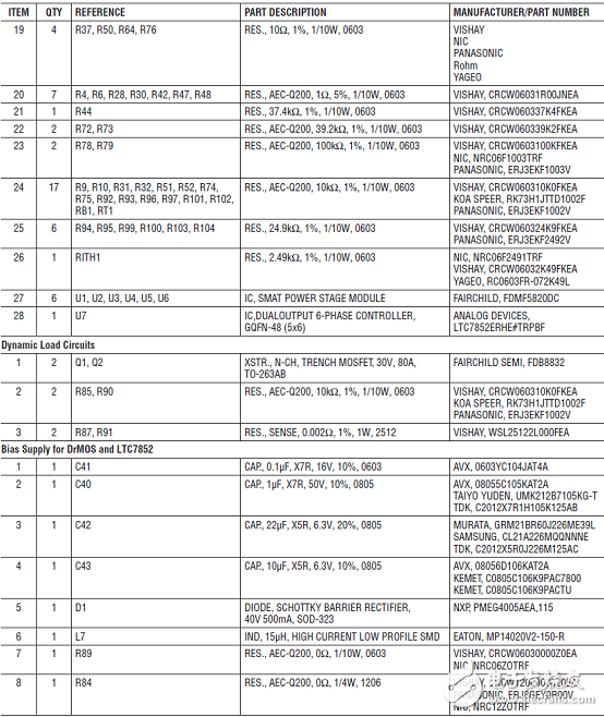
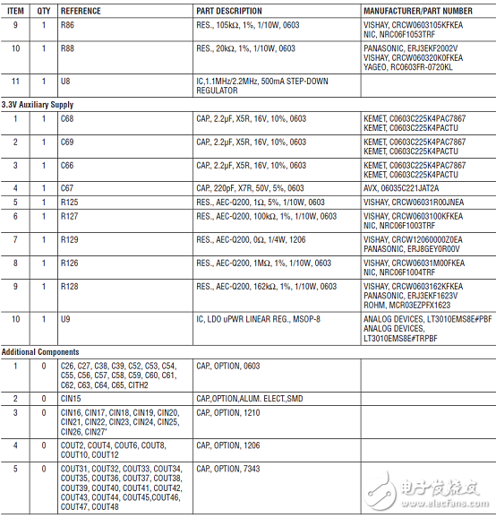
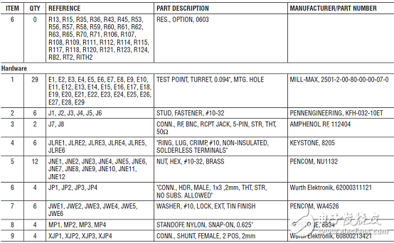
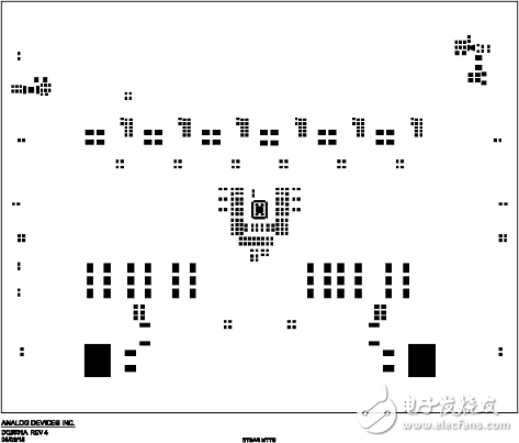
图10.演示板DC2631A PCB设计图(1)
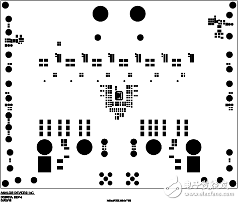
图11.演示板DC2631A PCB设计图(2)
图12.演示板DC2631A PCB设计图(3)
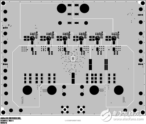
图13.演示板DC2631A PCB设计图(4)
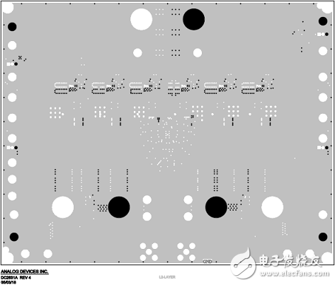
图14.演示板DC2631A PCB设计图(5)
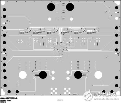
图15.演示板DC2631A PCB设计图(6)
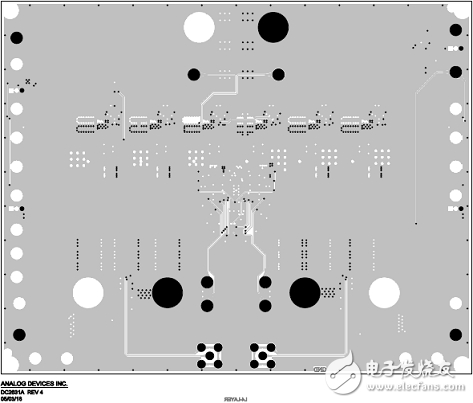
图16.演示板DC2631A PCB设计图(7)
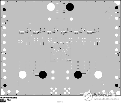
图17.演示板DC2631A PCB设计图(8)
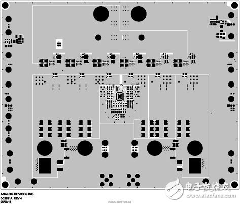
图18.演示板DC2631A PCB设计图(9)
-
深入解析LTC3862 - 1:多相电流模式升压DC/DC控制器的卓越性能与应用2026-03-12 509
-
深入剖析LTC3862 - 2:多相电流模式升压DC/DC控制器的卓越之选2026-03-10 394
-
LTC3774:高性能双路多相电流模式同步控制器的深度解析2026-03-09 371
-
LTC3862-2项目-多相电流模式升压DCDC控制器(6-36V至50V@10A)2021-05-30 955
-
LTC3774:用于亚百万欧姆DCR传感的双相多相电流模式同步控制器数据表2021-05-14 782
-
LTC3862:多相电流模式升压DC/DC控制器数据表2021-05-13 1106
-
LTC3862-2:多相电流模式升压DC/DC控制器数据表2021-05-12 982
-
LTC3862-1:多相电流模式升压DC/DC控制器数据表2021-04-24 961
-
LTC7852/LTC7852-1:带电流监测数据表的双输出6相多相电流模式同步控制器2021-03-22 902
-
用于 mΩ 以下 DCR 检测的双输出多相电流模式同步降压型 DC/DC 控制器2021-03-20 1036
-
LTC3773 - 三输出、三相电流模式降压型控制器2021-03-19 1072
-
电流模式双输出同步降压型DC/DC控制器LTC37742018-11-29 1886
-
双输出、多相降压型DC/DC控制器2010-02-23 1354
全部0条评论

快来发表一下你的评论吧 !
