

基于UCC21225A隔离双路栅极驱动和参考设计
电子说
描述
TI公司的ucc21225A是隔离双路栅极驱动器,具有源电流4A和沉峰值电流6A,封装为5-mm x 5-mm LGA-13.可以驱动高达5MHz的功率晶体管,具有业界最低的时延和脉宽失真。典型的传输时延为19ns,最大时延匹配为5ns,脉宽失真最大为6ns.两个次级边驱动器间内部功能隔离允许工作电压高达700V,可配置成两个低边,两个高边,或有可编死区时间(DT)的半桥驱动器,器件的VDD电源电压高达25V,宽输入VCCI范围从3V到18V,使得驱动非常适合于模拟和数字控制器间的接口,所有的电源引脚有欠压锁住(UVLO)保护。相关的安全规范包括3535-VPK Isolation per DIN V VDE V 0884-11:2017-01和2500-VRMS Isolation for 1 Minute per UL 1577.主要用在服务器,通信,IT和工业领域,DC/DC转换器和AC/DC转换器,马达驱动和DC/AC太阳能逆变器以及HEV和BEV电池充电器。本文介绍了UCC21225A主要特性,框图和功能框图,典型应用电路图以及10kW三级三相连接电网的太阳能逆变器参考设计TIDA-0160610-kW主要特性和指标,框图,电路图和材料清单。
The UCC21225A is an isolated dual-channel gatedriver with 4-A source and 6-A sink peak current in a5-mm x 5-mm LGA-13 package. It is designed todrive power transistors up to 5-MHz with best-in-classpropagation delay and pulse-width distortion.
The input side is isolated from the two output driversby a 2.5-kVRMS isolation barrier, with 100-V/nsminimum common-mode transient immunity (CMTI)。
Internal functional isolation between the twosecondary side drivers allows working voltage up to700-VDC.This driver can be configured as two low-side, twohigh-side, or a half-bridge driver with programmabledead time (DT)。 A disable pin shuts down bothoutputs simultaneously when it is set high, and allowsnormal operation when left open or grounded.
The device accepts VDD supply voltages up to 25-V.A wide input VCCI range from 3-V to 18-V makes thedriver suitable for interfacing with both analog anddigital controllers. All the supply voltage pins haveunder voltage lock-out (UVLO) protection.
With all these advanced features, the UCC21225Aenables high power density, high efficiency, androbustness in a wide variety of power applications.
UCC21225A主要特性:
1• Universal: Dual Low-Side, Dual High-Side or Half-Bridge Driver
• 5 x 5 mm, Space-Saving LGA-13 Package
• Switching Parameters:
– 19-ns Typical Propagation Delay
– 5-ns Maximum Delay Matching
– 6-ns Maximum Pulse-Width Distortion
• CMTI Greater than 100-V/ns
• 4-A Peak Source, 6-A Peak Sink Output
• TTL and CMOS Compatible Inputs
• 3-V to 18-V Input VCCI Range
• Up to 25-V VDD with 5-V UVLO
• Programmable Overlap and Dead Time
• Rejects Input Transients Shorter than 5-ns
• Fast Disable for Power Sequencing
• Safety-Related Certifications:
– 3535-VPK Isolation per DIN V VDE V 0884-11:2017-01
– 2500-VRMS Isolation for 1 Minute per UL 1577
– CQC per GB4943.1-2011 (Planned)
UCC21225A应用:
• Server, Telecom, IT and Industrial Infrastructures
• DC-DC and AC-to-DC Power Supplies
• Motor Drive and DC-to-AC Solar Inverters
• HEV and BEV Battery Chargers

图1. UCC21225A框图

图2. UCC21225A功能框图

图3. UCC21225A典型应用电路图
10kW三级三相连接电网太阳能逆变器的参考设计TIDA-0160610-kW
This reference design provides an overview on how toimplement a three-level, three-phase, SiC-basedDC/AC grid-tie inverter stage. A higher switchingfrequency of 50 kHz reduces the size of magnetics forthe filter design and as a result a higher power density.SiC MOSFETs with switching loss ensures higher DCbus voltages of up to 1000 V and lower switchinglosses with a peak efficiency of 99%. This design isconfigurable to work as a two-level or three-levelinverter.
参考设计TIDA-0160610-kW主要特性:
• Rated Nominal and Max Input Voltage at 800-Vand 1000-V DC
• Max 10-kW/10-kVA Output Power at 400-V AC50- or 60-Hz Grid-Tie Connection
• Operating Power Factor Range From 0.7 Lag to0.7 Lead
• High-Voltage (1200-V) SiC MOSFET-Based Full-Bridge Inverter for Peak Efficiency of 98.5%
• Compact Output Filter by Switching Inverter at50 kHz
• 《2% Output Current THD at Full Load
•Isolated Driver ISO5852S With Reinforced Isolationfor Driving High-Voltage SiC MOSFET andUCC5320S for Driving Middle Si IGBT
• Isolated Current Sensing Using AMC1301 for LoadCurrent Monitoring
• TMS320F28379D Control Card for Digital Control
参考设计TIDA-0160610-kW应用:
• Solar String Inverters
• Solar Central Inverters
图4.参考设计TIDA-0160610-kW外形图
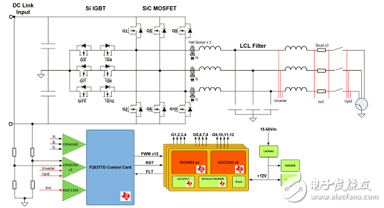
图5.参考设计TIDA-0160610-kW框图
参考设计TIDA-0160610-kW主要指标:


图6.二级三相逆变器架构图

图7.二级单相逆变器腿图

图8.三级T型三相逆变器架构图

图9.参考设计TIDA-0160610-kW电路图(1):逆变器栅极驱动器

图10.参考设计TIDA-0160610-kW电路图(2):逆变器栅极驱动器

图11.参考设计TIDA-0160610-kW电路图(3):ISO HV卡

图12.参考设计TIDA-0160610-kW电路图(4):ISO HV卡

图13.参考设计TIDA-0160610-kW电路图(5):ISO HV卡

图14.参考设计TIDA-0160610-kW电路图(6):电源控制卡

图15.参考设计TIDA-0160610-kW电路图(7):电源控制卡

图16.参考设计TIDA-0160610-kW电路图(8):电源控制卡

图17.参考设计TIDA-0160610-kW电路图(9):电源控制卡
-
探索UCC21225AEVM - 365评估模块的奥秘2026-07-08 131
-
解析UCC20520:高性能隔离双路栅极驱动器的技术探秘2026-01-23 523
-
UCC20225-Q1与UCC20225A-Q1:汽车48V系统隔离双路栅极驱动器的卓越之选2026-01-22 2316
-
UCC21231:高性能双路隔离栅极驱动器的技术解析与应用指南2026-01-20 627
-
UCC21225A 4 - A, 6 - A, 2.5 - kVRMS 隔离双通道栅极驱动器深度解析2026-01-09 1743
-
UCC21540-Q1隔离双路栅极驱动器:设计与应用全解析2026-01-08 662
-
LGA中的4-A、6-A、2.5kVRMS隔离双通道栅极驱动器UCC21225A数据表2024-04-08 557
-
电源和电机驱动的两种MOS的冗余驱动线路2022-01-18 4087
-
UCC21225A 采用 LGA 封装的 4A/6A 2.5kVRMS 隔离式双通道栅极驱动器2018-10-16 413
全部0条评论

快来发表一下你的评论吧 !
