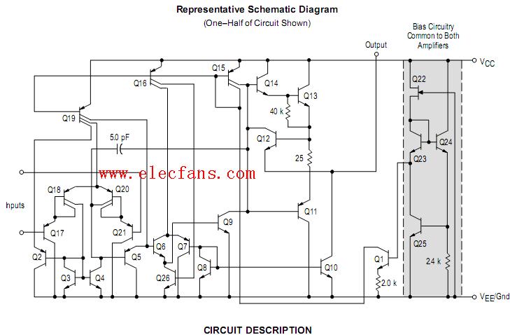

lm358内部电路图
IC应用电路图
描述
lm358内部电路图
The LM258 series is made using two internally
compensated, two–stage operational amplifiers. The first
stage of each consists of differential input devices Q20 and
Q18 with input buffer transistors Q21 and Q17 and the
differential to single ended converter Q3 and Q4. The first
stage performs not only the first stage gain function but also
performs the level shifting and transconductance reduction
functions. By reducing the transconductance, a smaller
compensation capacitor (only 5.0 pF) can be employed, thus
saving chip area. The transconductance reduction is
accomplished by splitting the collectors of Q20 and Q18.
Another feature of this input stage is that the input common
mode range can include the negative supply or ground, in
single supply operation, without saturating either the input
devices or the differential to single–ended converter. The
second stage consists of a standard current source load
amplifier stage.
Each amplifier is biased from an internal–voltage regulator
which has a low temperature coefficient thus giving each
amplifier good temperature characteristics as well as
excellent power supply rejection.
-
bigboy1010 2012-10-19
0 回复 举报好 收起回复
- 相关推荐
- 热点推荐
- LM358
-
lm358碱性电池充电器电路图2014-05-20 13276
-
LM358典型应用电路图 双运算放大器电路设计2023-07-17 26651
-
什么原因会引起LM358芯片内部电路短路?2024-08-16 1710
-
LM358电路组成的麦克风电路原理图2011-12-16 39225
-
lm3582013-05-11 3135
-
LM358的电压跟随器与运放问题2018-08-29 11806
-
lm358恒流源电路2008-01-31 29132
-
lm358电路原理图2008-06-16 30828
-
基于LM358放大器的比较电路图2010-08-25 28749
-
LM358的原理图2016-03-23 3471
-
lm358引脚图及功能说明2016-09-22 705619
-
lm358中文资料汇总(lm358引脚图及功能_工作原理及应用电路讲解)2018-05-22 574849
-
LM358典型应用电路图集2021-06-11 6296
-
LM358镍氢电池充电器电路图2022-03-04 4486
-
lm358电压上限和下限比较 LM358和LM358P区别是什么2024-01-28 19498
全部0条评论

快来发表一下你的评论吧 !


