

浅谈TI TPS546D24A四相160A同步降压转换器参考设计PMP21814
应用案例
描述
TI公司的TPS546D24A是高度集成非隔离DC/DC转换器,具有高频工作,输出电流40A,封装为7mmx5mm 40引脚QFN封装.两个,三个和四个TPS546D24A可以互连,单输出可提供高达160A输出.TPS546D24A采用专有的固定频率电流模式控制,具有输入正馈和可选择的内部补偿元件,以最小化尺寸和大范围输出电容下稳定性.PMBus接口具有1MHz时钟,支持方便标准化的数字接口,用于转换器配置和监视主要参数包括输出电压,输出电流和内部芯片温度.器件分立的轨电压支持2,95V-16V PVIN;2.9V-18V AVIN,集成了4.5-mΩ/0.9-mΩ MOSFET,2×, 3x, 4×可堆栈共享电流高达160A,每个输出支持单地址.12个可选开关频率,从225 kHz 到1.5 MHz.主要用在数据中心交换,机架式服务器,有源天线系统,遥控无线电和基带单元,自动测试,CT,PET和MRI以及ASIC,SoC,FPGA,DSP核和I/O电压.中电网为您整理如下互联网详细资料本文介绍了TPS546D24A主要特性,功能框图,平均电流模式控制框图,单个和两个器件应用电路,以及两相降压转换器评估板TPS546D24AEVM-2PH主要特性和指标,电路图,材料清单,PCB设计图.以及四相160A同步降压转换器参考设计PMP21814框图,电路图,材料清单和PCB设计图.
The TPS546D24A is a highly integrated, non-isolatedDC/DC converter capable of high frequency operationand 40-A current output from a 7-mm × 5-mmpackage. Two, three, and four TPS546D24A devicescan be interconnected to provide up to 160 A on asingle output. The device has an option to overdrivethe internal 5-V LDO with an external 5-V supply viathe VDD5 pin to improve efficiency and reduce powerdissipation of the converter.
The TPS546D24A uses a proprietary fixed-frequencycurrent-mode control with input feedforward andselectable internal compensation components forminimal size and stability over a wide range of outputcapacitances.
The PMBus interface with 1-MHz clock support givesa convenient, standardized digital interface forconverter configuration as well as monitoring of keyparameters including output voltage, output current,and internal die temperature. Response to faultconditions can be set to restart, latch off, or ignore,depending on system requirements. Back-channelcommunication between stacked devices enables allTPS546D24A converters powering a single output railto share a single address to simplify systemsoftware/firmware design. Key parameters includingoutput voltage, switching frequency, soft-start time,and overcurrent fault limits can also be configuredthrough BOM selection without PMBuscommunication to support program free power-up.
TPS546D24A主要特性:
• Split rail support: 2.95-V to 16-V PVIN;2.95-V to 18-V AVIN (4-VIN VDD5 for switching)
• Integrated 4.5-mΩ/0.9-mΩ MOSFETs
• Average current mode control with selectableinternal compensation
• 2×, 3x, 4× stackable with current sharing up to160 A, supporting a single address per output
• Selectable 0.6-V to 5.5-V output via pin strap or0.25-V to 6.0-V using PMBus VOUT_COMMAND
• Extensive PMBus command set with telemetry forVOUT, IOUT and internal die temperature
• Differential remote sensing with internal FB dividerfor < 1% VOUT error –40°C to +150°C TJ
• AVS and margining capabilities through PMBus
• MSEL pins pin programming PMBus defaults
• 12 Selectable switching frequencies from 225 kHzto 1.5 MHz (8 pin-strap options)
• Frequency sync in/sync out
• Supports prebiased output
• Supports strongly coupled inductor
• 7 mm × 5 mm × 1.5 mm, 40-pin QFN,Pitch = 0.5 mm
• Create a Custom Design Using the TPS546D24AWith WEBENCH® Power Designer
TPS546D24A应用:
• Data center switches, rack servers
• Active antenna system, remote radio andbaseband unit
• Automated test equipment, CT, PET, and MRI
• ASIC, SoC, FPGA, DSP core, and I/O voltage
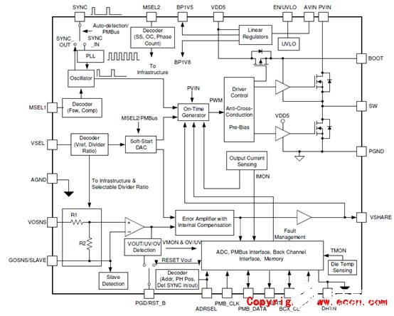
图1.TPS546D24A功能框图
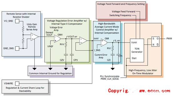
图2.TPS546D24A平均电流模式控制框图
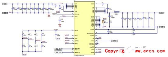
图3.TPS546D24A单个应用电路图
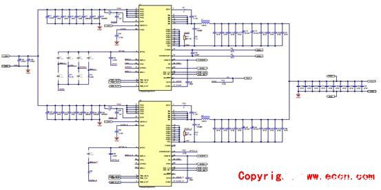
图4.TPS546D24A两相应用电路图
两相降压转换器评估板TPS546D24AEVM-2PH
The TPS546D24AEVM-2PH evaluation module (EVM) is a two-phase buck converter with twoTPS546D24A devices. The TPS546D24A device is a stackable synchronous buck with PMBus interfacethat can operate from a nominal 2.95-V to 16-V supply. The device allows programming and monitoringvia the PMBus interface.
Two TPS546D24A devices are configured as two-phase buck converter in factory default, output current isevenly distributed in the two devices; both the negative and positive output terminals are connectedtogether.designed for a nominal 12-V bus and to produce a regulated 0.8-V output at up to 80 A of load current.
The TPS546D24AEVM-2PH is designed to demonstrate stacking operation of the TPS546D24A in a twophase,low-output voltage application while providing a number of test points to evaluate the performanceof the devices. The TPS546D24AEVM-2PH can be modified to single-phase buck converters by changingthe components assembled.
评估板TPS546D24AEVM-2PH主要特性:
• Regulated 0.8-V output up to 80-ADC steady-state output current
• The output voltage is marginable and trimmable using the PMBus interface
– Programmable UVLO, soft-start, and enable via the PMBus interface
– Programmable overcurrent warning and fault limits and programmable response to faults via thePMBus interface
– Programmable overvoltage and undervoltage warning and fault limits and programmable responseto faults via the PMBus interface
– Programmable turn-on and turn-off delays
• Convenient test points for probing critical waveforms
The TPS546D24A device is designed for the following applications:
• High-density power solutions
• Wireless infrastructure
• Switcher
• Router network
• Server
• Storage
• Smart power systems
评估板TPS546D24AEVM-2PH主要电指标:
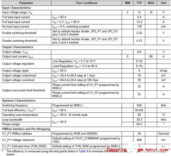
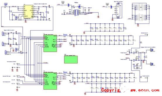
图5.评估板TPS546D24AEVM-2PH电路图(1)
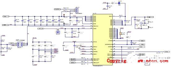
图6.评估板TPS546D24AEVM-2PH电路图(2)(U1 P1主)
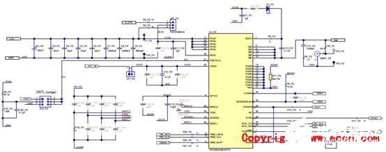
图7.评估板TPS546D24AEVM-2PH电路图(3)(U1_P2从)
评估板TPS546D24AEVM-2PH材料清单:
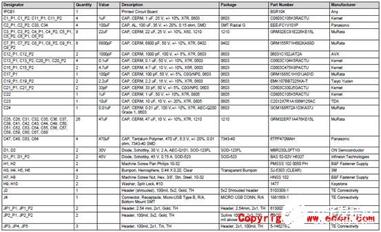
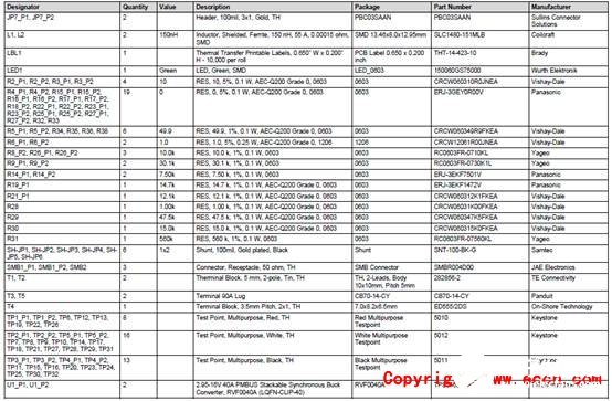
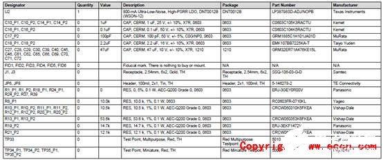
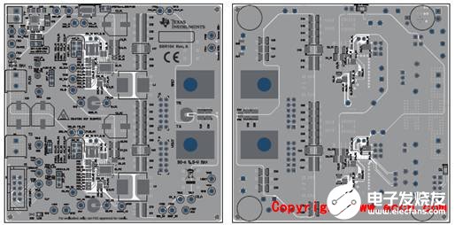
图8.评估板TPS546D24AEVM-2PH PCB设计图:左:顶层元件;右:底层元件
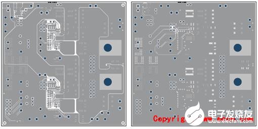
图9.评估板TPS546D24AEVM-2PH PCB设计图:左:顶层铜;右:内层1
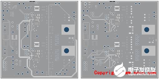
图10.评估板TPS546D24AEVM-2PH PCB设计图:左:内层2;右:内层3
图11.评估板TPS546D24AEVM-2PH PCB设计图:左:内层4;右:内层5
图12.评估板TPS546D24AEVM-2PH PCB设计图:左:内层6;右:内底层
四相160A同步降压转换器参考设计PMP21814
PMP21814 4-phase, 160-ASynchronous Buck Converter ReferenceDesign for Communications Processor Power
This reference design uses four TPS546D24A converters with integrated MOSFETs to support a full load of 160-A at a 0.9-V output. The system operates at a switching frequency of 650 kHz and has a PMBus interface thatcan be used to configure key converter parameters, including internal compensation. The detailed test reportincludes efficiency, thermal, stability, and load transient results.
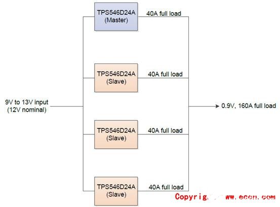
图13.四相160A同步降压转换器PMP21814参考设计框图
图14.四相160A同步降压转换器PMP21814参考设计外形图(正面)
图15.四相160A同步降压转换器PMP21814参考设计外形图(背面)
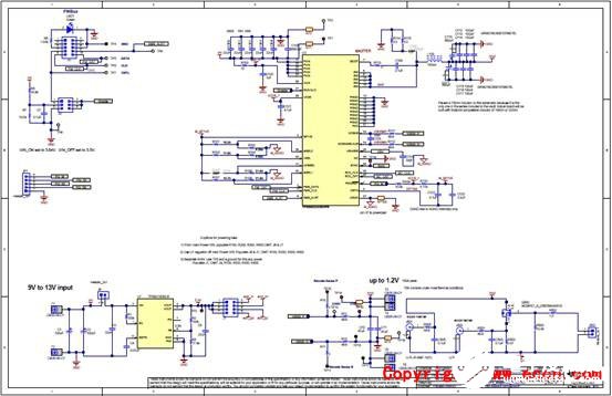
图16.四相160A同步降压转换器PMP21814参考设计电路图(1)
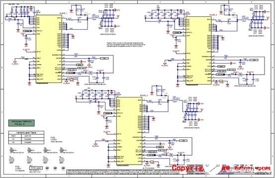
图17.四相160A同步降压转换器PMP21814参考设计电路图(2)
PMP21814 REV材料清单:
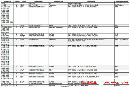
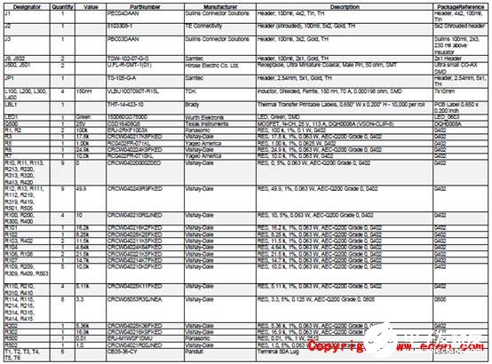
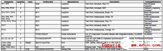
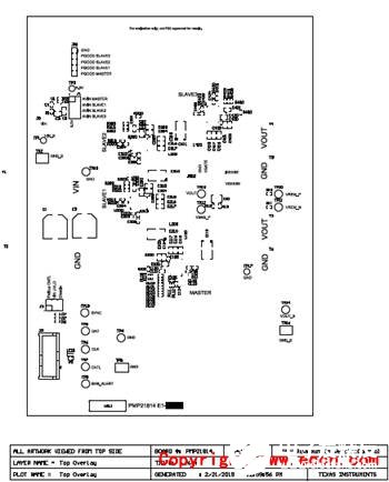
图18.四相160A同步降压转换器PMP21814参考设计PCB设计图(1)
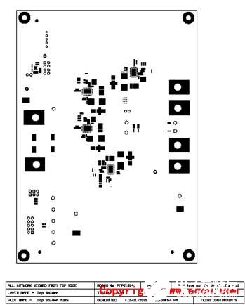
图19.四相160A同步降压转换器PMP21814参考设计PCB设计图(2)
图20.四相160A同步降压转换器PMP21814参考设计PCB设计图(3)
图21.四相160A同步降压转换器PMP21814参考设计PCB设计图(4)
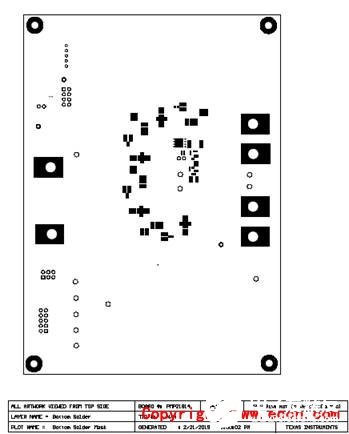
图22.四相160A同步降压转换器PMP21814参考设计PCB设计图(5)
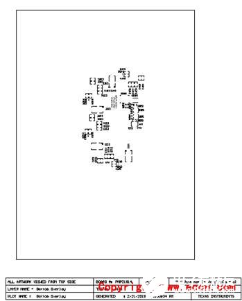
图23.四相160A同步降压转换器PMP21814参考设计PCB设计图(6)
图24.四相160A同步降压转换器PMP21814参考设计PCB设计图(7)
图25.四相160A同步降压转换器PMP21814参考设计PCB设计图(8)
-
TPS546D24A PMBUSTM输出电压和输出电流介绍2022-11-04 664
-
开源硬件-PMP21814.1-适用于通信处理器电源的四相、160A 同步降压转换器 PCB layout 设计2010-03-18 2272
-
TI推出新型40-A SWIFTTM DC/DC降压转换器,可在高开关频率下提高效率2020-03-11 4766
-
德州仪器为实现功率密度更大化推出堆栈式DC/DC降压转换器2020-03-12 3750
-
具有PMBus接口的高密度160A 4相DC DC降压转换器设计2022-09-08 745
-
TPS546D24A PMBUSTM输出电压和输出电流2022-10-28 783
-
PMP21254.1-具有集成 FET 控制器的 160A 四相 PCB layout 设计2024-05-19 431
-
2.95V至16V、40A、高达4×可堆叠、PMBus® 降压转换器TPS546D24A数据表2024-04-03 532
-
使用TPS546D24A实现优于1%的输出电压精度2024-08-26 405
-
TPS546A24A SWIFT™降压转换器评估模块用户指南2024-11-16 470
-
TPS546D24A两相SWIFT™降压转换器评估模块用户指南2024-11-18 646
-
TPS546D24A 具有引脚搭接和 PMBus® 的 2.95V 至 16V、可堆叠 40A 同步 SWIFT™ 降压转换器数据手册2025-06-12 1440
-
TPS546A24S同步降压转换器技术解析与应用指南2025-08-08 1253
-
德州仪器TPS546D24SEVM-2PH评估模块技术解析与应用指南2025-08-25 2019
-
TPS546D24S同步降压转换器技术解析与应用指南2025-08-26 1172
全部0条评论

快来发表一下你的评论吧 !
