
WLAN Reference Design with the
通信设计应用
65人已加入
描述
WLAN Reference Design with the MAX2830
Abstract: This reference design is a complete RF front-end solution designed to meet the WLAN IEEE® 802.11b/g standard. Using the MAX2830 RF transceiver, the design is capable of accommodating full range of 802.11g OFDM data rates (6, 9, 12, 18, 24, 36, 48, and 54Mbps) and 802.11b QPSK data rates (1, 2, 5.5, and 11Mbps). This solution offers high performance, small size, and low BOM cost.
Figure 1. The WLAN reference design features the MAX2830 RF transceiver.
| Important Design Features |
- High-Performance Rx NF < 6dB (typ); Tx Output 15dBm (typ)
- Small Size: 17mm x 24.7mm
- Platform Design for Multiple Form-Factors such as Card Bus and Compact Flash

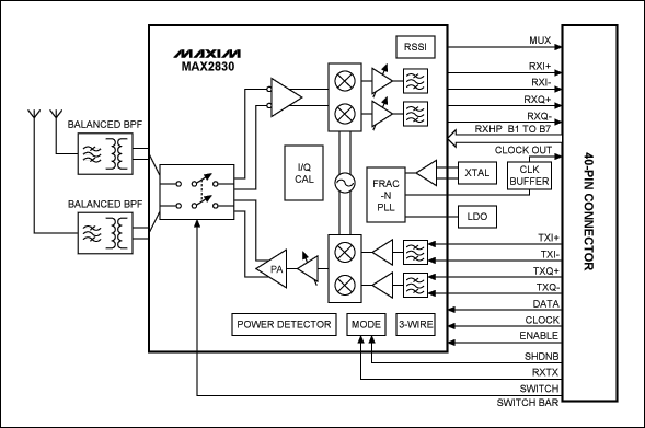
Figure 2. Block diagram of the WLAN reference design.
| Lab Measurements |
| ||||||||||||||||||||||||||||||||||||||||||||||||||||||||||||||||||||||||||||||||||||||||||||||||||||||||
| Operating Characteristics |

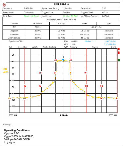
Figure 3. ACPR performance at Tx power = 15.7dBm, EVM < 5.6%.

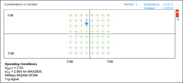
Figure 4. Rx I/Q constellation diagram at RF input = -40dBm, 54Mbps 64QAM, EVM = 2.2%.
Figure 5. Rx I/Q constellation diagram at PIN = -65dBm, 54Mbps 64QAM. The EVM is only 4.2%, which is better than the 9% requirement for sensitivity.
| Detailed Description |
This reference design is suitable for the full range of 802.11g OFDM data rates (6, 9, 12, 18, 24, 36, 48, and 54Mbps) and 802.11b QPSK data rates (1, 2, 5.5, and 11Mbps) at corresponding sensitivity levels. Using the MAX2830 chipset eliminates the need for external SAW filters, a RF switch, and a PA. Only a RF filter, RF balun, and a small number of passive components are required to form a complete 11b/g WLAN RF front-end solution that delivers high performance in a small PCB form-factor.
IEEE is a registered service mark of the Institute of Electrical and Electronics Engineers.
声明:本文内容及配图由入驻作者撰写或者入驻合作网站授权转载。文章观点仅代表作者本人,不代表电子发烧友网立场。文章及其配图仅供工程师学习之用,如有内容侵权或者其他违规问题,请联系本站处理。
举报投诉
- 相关推荐
- 热点推荐
- WLAN
-
Base Targeted Reference Design (TRD)2015-07-01 3662
-
Reference Design Report for a2009-06-28 667
-
LED Reference Design Kit2009-10-23 738
-
Transmitter Reference Design f2008-08-18 1348
-
WiBro Reference Design with th2008-09-17 1357
-
Reference Design Ensures Dynam2009-03-23 1203
-
Reference Design for Power-ove2009-04-23 1471
-
Reference Design for a High-Cu2009-05-02 1879
-
Reference Design for a Signal-2009-06-30 1348
-
Reference Design for a PC-Base2009-09-27 1167
-
Reference Design for a High-In2009-11-08 1703
-
arduino_Due_Reference_design2016-01-11 942
-
AD4020 Reference Design Software2021-01-31 851
-
Design Files for FCC Part 90 Reference Design2021-02-01 1059
-
Eterna Extended Range Reference Design2021-02-21 800
全部0条评论

快来发表一下你的评论吧 !

