
Accurate DC-DC Converter Minim
电源设计应用
455人已加入
描述
Whether squeezing the last millijoule from your battery or operating a cooler CPU board, the goal is to burn less power. For many loads the power dissipation varies as the square of the applied voltage, so one approach is simply to minimize the supply voltage. Power dissipation equals V²/R in a resistive load and CV²F in a CMOS load, where C is the internal CMOS capacitance and F is the frequency.
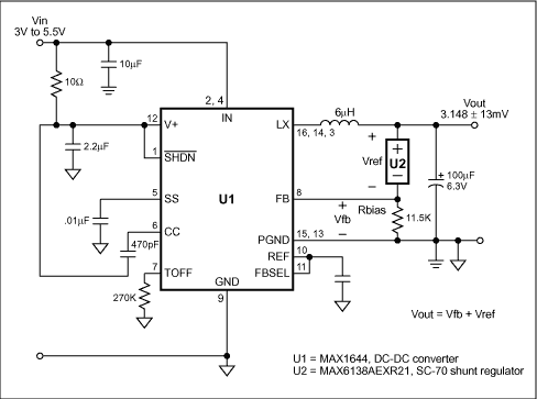
The consequence of this square law dependency is a 2% change in power dissipation for every 1% change in voltage. Clearly, tight power control is a consequence of tight voltage control. To achieve that goal, the circuit of Figure 1 produces an output voltage whose accuracy is far tighter than that of the DC-DC converter's internal voltage, and without need for precision external resistors.

Figure 1. Substituting a shunt regulator (U2) for the customary resistive divider in this DC-DC converter dramatically improves the output voltage accuracy.
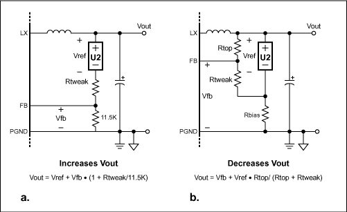
To determine the optimum supply voltage, you must consider the circuit's minimum voltage requirement, the DC-DC converter's output ripple and line/load regulation, and any voltage drops between the converter and its load(s). One would ideally set the power-supply output to the resulting minimum, but actual DC-DC converters have non-ideal references whose percent error appears directly in the output. The tolerances on discrete-valued external resistors also contribute an output voltage error. The circuit of Figure 1 (and the modifications shown in Figure 2) describe a technique that almost eliminates the potentially significant errors contributed by a resistive feedback divider. It also minimizes error due to variation in the internal reference voltage.

Figure 2. To adjust the output voltage, add Rtweak to the Figure 1 circuit to either increase Vout (a) or decrease Vout (b), as indicated by the equations.
The Figure 1 circuit is that of the MAX1644 Evaluation Kit, except that the output divider has been replaced with bias resistor Rbias and a 0.1%-accurate 2.048V shunt regulator (U2). The DC-DC converter's output voltage is the sum of the shunt voltage and the internal reference voltage at the feedback point. The MAX1644 reference voltage is 1.10V ± 11mV (which is ±1%), and the MAX6138 shunt reference voltage is 2.048V ±2mV. The circuit's output voltage is therefore 3.148V ±13 mV (which is ±0.4%). If we assume that output power varies as the square of the voltage, then it varies by ±0.8%, which is a range of 1.6%.
Note that the output-voltage accuracy (±0.4%) is better than the DC-DC converter's reference-voltage accuracy (±1%). That result cannot be achieved with a resistor string, even one with perfect resistors, nor can it be achieved even with the output tied directly to the internal reference.
An output of 3.148V -0.4% is almost exactly 3.3V -5%, which may be optimum for many 3.3V systems. For other values of output voltage, consider Figures 2a and 2b. Figure 2a adds a resistor (Rtweak) in series with the shunt reference, thereby raising the output voltage by an amount VFB × Rtweak/11.5kΩ. If Rtweak is small it will have a negligible effect on output voltage accuracy. If the output voltage is too high, you can lower it using the circuit of Figure 2b. Here again, small values of Rtweak will have a negligible effect on output voltage accuracy. Note that the Rbias value should be small enough to provide for U2 a minimum bias current of 65µA.
To compare the output accuracy of Figure 1 with that of a 3.148V DC-DC converter featuring a simple resistive divider in the feedback path (Table 1), consider a 143k/76.8k divider using 1% resistors. Assuming a 1.1V reference in the converter IC, the worst-case variation in output voltage due to the resistor tolerance is approximately ±1.3%. Any variation in the reference (±1%, in this case) is seen directly in the output voltage. Thus, adding the two independent sources of error (±1.3% and ±1%) yields an output-voltage variation of ±2.3%, producing a power variation of ±4.6% (a range of 9.2%).
Table 1 3.148V DC-DC converter featuring 1% resistor divider vs. 0.1% shunt
A sensitivity analysis of the resistor-divider circuit reveals why its power range is more than five times that of the shunt circuit:

where Rtop is the top resistor, Rbot is the bottom resistor, and Vfb is the internal reference voltage.
The above equation relates the fractional change in Vout to fractional changes in Rtop, Rbot and Vfb. If Rtop = Rbot, for example, then a +1% change in Rtop causes a +0.5% change in Vout. Note that a 1% change in Vfb causes a 1% change in Vout that is independent of the resistor values. The equation demonstrates that even with perfect resistors (dRtop = dRbot = 0) the fractional change in output voltage can never be better than the fractional change in Vfb. When using a resistor divider, the output-voltage accuracy can never be better than the accuracy of the DC-DC converter's internal reference. Resistor errors can only worsen the accuracy.
The output voltage of Figure 1 has no resistor sensitivity. What's more, the shunt reference acts as a level translator. If Vfb has an error of ±11mV, the error translates directly to the output, where it appears as a ±1% error of the 1.1V internal reference, not of the output voltage. That is the beauty of this arrangement: the ±11mV error is only ±0.35% of the 3.148V output.
Changing the shunt can accommodate other output voltages. The 2.048V shunt provides 3.3V -5%, and a 1.2205V shunt (MAX6138AEXR12) generates an output voltage of 2.3205V, which is 2.5V -7.2%. The circuits of Figures 2a and 2b can introduce minor adjustments if necessary. Other shunt reference voltages can be used for other output voltage requirements.
The circuit of Figure 1 was tested with a 1.2205V reference and then with a 2.048V reference, applying DC tests with different loads and AC tests with a dynamic load under various static and dynamic conditions. The circuit exhibited a fast response with no overshoot or ringing, and was stable without use of additional compensation. The turn-on transients were also well-behaved under various load conditions. All tests were conducted with the FBSEL pin connected to the reference (as shown in Figure 1), and then with the FBSEL pin connected to ground. For highly accurate outputs that improve the output load regulation by 50%, connect the FBSEL pin to ground.
These simple circuits can provide surprisingly large savings in power dissipation and battery life.
打开APP阅读更多精彩内容
The consequence of this square law dependency is a 2% change in power dissipation for every 1% change in voltage. Clearly, tight power control is a consequence of tight voltage control. To achieve that goal, the circuit of Figure 1 produces an output voltage whose accuracy is far tighter than that of the DC-DC converter's internal voltage, and without need for precision external resistors.

Figure 1. Substituting a shunt regulator (U2) for the customary resistive divider in this DC-DC converter dramatically improves the output voltage accuracy.
To determine the optimum supply voltage, you must consider the circuit's minimum voltage requirement, the DC-DC converter's output ripple and line/load regulation, and any voltage drops between the converter and its load(s). One would ideally set the power-supply output to the resulting minimum, but actual DC-DC converters have non-ideal references whose percent error appears directly in the output. The tolerances on discrete-valued external resistors also contribute an output voltage error. The circuit of Figure 1 (and the modifications shown in Figure 2) describe a technique that almost eliminates the potentially significant errors contributed by a resistive feedback divider. It also minimizes error due to variation in the internal reference voltage.

Figure 2. To adjust the output voltage, add Rtweak to the Figure 1 circuit to either increase Vout (a) or decrease Vout (b), as indicated by the equations.
The Figure 1 circuit is that of the MAX1644 Evaluation Kit, except that the output divider has been replaced with bias resistor Rbias and a 0.1%-accurate 2.048V shunt regulator (U2). The DC-DC converter's output voltage is the sum of the shunt voltage and the internal reference voltage at the feedback point. The MAX1644 reference voltage is 1.10V ± 11mV (which is ±1%), and the MAX6138 shunt reference voltage is 2.048V ±2mV. The circuit's output voltage is therefore 3.148V ±13 mV (which is ±0.4%). If we assume that output power varies as the square of the voltage, then it varies by ±0.8%, which is a range of 1.6%.
Note that the output-voltage accuracy (±0.4%) is better than the DC-DC converter's reference-voltage accuracy (±1%). That result cannot be achieved with a resistor string, even one with perfect resistors, nor can it be achieved even with the output tied directly to the internal reference.
An output of 3.148V -0.4% is almost exactly 3.3V -5%, which may be optimum for many 3.3V systems. For other values of output voltage, consider Figures 2a and 2b. Figure 2a adds a resistor (Rtweak) in series with the shunt reference, thereby raising the output voltage by an amount VFB × Rtweak/11.5kΩ. If Rtweak is small it will have a negligible effect on output voltage accuracy. If the output voltage is too high, you can lower it using the circuit of Figure 2b. Here again, small values of Rtweak will have a negligible effect on output voltage accuracy. Note that the Rbias value should be small enough to provide for U2 a minimum bias current of 65µA.
To compare the output accuracy of Figure 1 with that of a 3.148V DC-DC converter featuring a simple resistive divider in the feedback path (Table 1), consider a 143k/76.8k divider using 1% resistors. Assuming a 1.1V reference in the converter IC, the worst-case variation in output voltage due to the resistor tolerance is approximately ±1.3%. Any variation in the reference (±1%, in this case) is seen directly in the output voltage. Thus, adding the two independent sources of error (±1.3% and ±1%) yields an output-voltage variation of ±2.3%, producing a power variation of ±4.6% (a range of 9.2%).
Table 1 3.148V DC-DC converter featuring 1% resistor divider vs. 0.1% shunt
|
Vout/Vref
|
Vout error due to DC-DC ref. error |
Vout error due to ±1% resistors |
Vout error due to shunt ref. error |
Total Vout error |
Total load-power error |
Total load-power range | |
|
With 1% resistor string |
3.148 /1.1 |
±31.5mV = ± 1.0% |
~±41mV = ± 1.3% |
0 |
± 72.5mV = ± 2.3% |
± 4.6% |
9.2% |
|
With 0.1% shunt |
3.148 /1.1 |
± 11mV = ± 0.35% |
0 |
± 2mV = ± 0.064% |
± 13mV = ± 0.41% |
± 0.82% |
1.64% |
A sensitivity analysis of the resistor-divider circuit reveals why its power range is more than five times that of the shunt circuit:

where Rtop is the top resistor, Rbot is the bottom resistor, and Vfb is the internal reference voltage.
The above equation relates the fractional change in Vout to fractional changes in Rtop, Rbot and Vfb. If Rtop = Rbot, for example, then a +1% change in Rtop causes a +0.5% change in Vout. Note that a 1% change in Vfb causes a 1% change in Vout that is independent of the resistor values. The equation demonstrates that even with perfect resistors (dRtop = dRbot = 0) the fractional change in output voltage can never be better than the fractional change in Vfb. When using a resistor divider, the output-voltage accuracy can never be better than the accuracy of the DC-DC converter's internal reference. Resistor errors can only worsen the accuracy.
The output voltage of Figure 1 has no resistor sensitivity. What's more, the shunt reference acts as a level translator. If Vfb has an error of ±11mV, the error translates directly to the output, where it appears as a ±1% error of the 1.1V internal reference, not of the output voltage. That is the beauty of this arrangement: the ±11mV error is only ±0.35% of the 3.148V output.
Changing the shunt can accommodate other output voltages. The 2.048V shunt provides 3.3V -5%, and a 1.2205V shunt (MAX6138AEXR12) generates an output voltage of 2.3205V, which is 2.5V -7.2%. The circuits of Figures 2a and 2b can introduce minor adjustments if necessary. Other shunt reference voltages can be used for other output voltage requirements.
The circuit of Figure 1 was tested with a 1.2205V reference and then with a 2.048V reference, applying DC tests with different loads and AC tests with a dynamic load under various static and dynamic conditions. The circuit exhibited a fast response with no overshoot or ringing, and was stable without use of additional compensation. The turn-on transients were also well-behaved under various load conditions. All tests were conducted with the FBSEL pin connected to the reference (as shown in Figure 1), and then with the FBSEL pin connected to ground. For highly accurate outputs that improve the output load regulation by 50%, connect the FBSEL pin to ground.
These simple circuits can provide surprisingly large savings in power dissipation and battery life.
声明:本文内容及配图由入驻作者撰写或者入驻合作网站授权转载。文章观点仅代表作者本人,不代表电子发烧友网立场。文章及其配图仅供工程师学习之用,如有内容侵权或者其他违规问题,请联系本站处理。
举报投诉
- 相关推荐
- 热点推荐
- C
-
DC-DC电源设计几点经验以及规则2023-04-08 1496
-
A 50W, 48V-to-5V DC-DC Converter Using the HIP21002009-05-12 3265
-
DC-DC基础入门教程 Advanced DC-DC Converters2009-10-31 40376
-
开关电源设计基础教程-DC/DC Converter2013-04-16 5940
-
关于DC-DC 转换器的问题,大师们,COME ON2014-12-22 3505
-
OBC与DC-DC开发测试过程2021-09-17 2685
-
LDO和DC-DC有什么不同?2021-11-17 1394
-
Low-Power DC-DC Converter Deri2009-04-30 787
-
1000Vdc Single & Dual Output 1 Watt Dc-Dc Converter2009-06-21 671
-
DC-DC 变压器2009-11-19 516
-
脉宽调制和DC - DC转换(PWM & DC-DC Con2009-11-20 720
-
减少DC-DC Converter中的地弹2010-06-07 784
-
Building a DC-DC power supply2010-09-23 2326
-
MAX731开关控制型DC-DC升压变换器,MAX731 DC-DC converter2018-09-20 2158
-
MAX20419: High-Efficiency, 3-Output, Low-Voltage DC-DC Converter Data Sheet MAX20419: High-Efficiency, 3-Output, Low-Voltage DC-DC Converter2023-10-16 78
全部0条评论

快来发表一下你的评论吧 !

