
Build High-GBW Op-Amp From A D
视频技术
16人已加入
描述
Abstract: Build a composite amplifier featuring high gain, wide bandwidth, good DC accuracy and low distortion by cascading a dual amplifier and adding phase compensation.
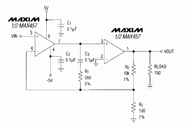
You can build a composite amplifier featuring high gain, wide bandwidth, and good DC accuracy by cascading the sections of a dual video amplifier and adding two appropriate phase-compensation components. In the example shown (Figure 1) the op amp drives a 150Ω load and provides a closed-loop gain of 40dB. You can obtain 40dB by cascading two 20dB sections, but that arrangement allows significant output distortion. (The video amplifiers normally operate at low gain while driving 75Ω or 150Ω loads.
The individual video amplifiers are unity-gain stable without external compensation, and have unity-gains bandwidth of 72MHz. They operate on ±5V supplies and consume about 350mW as a pair. Other typical specs include 2mV input offset, 100pA input bias currents, -72dB isolation between amplifiers, and differential phase and gain errors of 0.2° and 0.5%. The dual-amplifier chip comes in an 8-lead DIP.

Figure 1. This composite amplifier, based on a dual video-amplifier IC, provides a 40dB gain and 10MHz bandwidth while driving a 150Ω load.Max457 pdf datasheet.
The approach taken in Figure 1 minimizes output distortion. The first amplifier, operating with no (DC) load, provides it's maximum voltage gain of about 660V/V. The second amplifier, drivng a 150Ω load, has a voltage gain of about 65. Total open-loopgain for the composite amplifiers is thus 660×65, or about 92dB. In the absence of phase-compensation componenets R1 and C3, however, the circuit will oscillate.
With the 150Ω load, output swing is typically ±3.3V and linearity (between -2V and 2V) is about ±0.5%. R1 and C3 adjust the -3dB frequency to 10MHz, giving a gain-bandwidth product of 1GHz. The amplifier provides a 2V output swing with only 3% peaking near the 10MHz rolloff frequency. For comparison, a BB3554 or AD3554 operating at 40dB with no phase compensation (for maximum bandwidth) has a -3dB bandwidth of only 7MHz.
Table 1. Input and output voltages.
(Offset voltage not adjusted)
The table in Figure 1 gives DC performance for the closed-loop amplifier. Gain resistors R2 and R3 measured 99.78 and 9965Ω, giving a theoretical gain of R2 + R3 / R3 = 1000.870V/V—which is very close to the value of 100.825 measured for range -2V to 2V.
打开APP阅读更多精彩内容
You can build a composite amplifier featuring high gain, wide bandwidth, and good DC accuracy by cascading the sections of a dual video amplifier and adding two appropriate phase-compensation components. In the example shown (Figure 1) the op amp drives a 150Ω load and provides a closed-loop gain of 40dB. You can obtain 40dB by cascading two 20dB sections, but that arrangement allows significant output distortion. (The video amplifiers normally operate at low gain while driving 75Ω or 150Ω loads.
The individual video amplifiers are unity-gain stable without external compensation, and have unity-gains bandwidth of 72MHz. They operate on ±5V supplies and consume about 350mW as a pair. Other typical specs include 2mV input offset, 100pA input bias currents, -72dB isolation between amplifiers, and differential phase and gain errors of 0.2° and 0.5%. The dual-amplifier chip comes in an 8-lead DIP.

Figure 1. This composite amplifier, based on a dual video-amplifier IC, provides a 40dB gain and 10MHz bandwidth while driving a 150Ω load.Max457 pdf datasheet.
The approach taken in Figure 1 minimizes output distortion. The first amplifier, operating with no (DC) load, provides it's maximum voltage gain of about 660V/V. The second amplifier, drivng a 150Ω load, has a voltage gain of about 65. Total open-loopgain for the composite amplifiers is thus 660×65, or about 92dB. In the absence of phase-compensation componenets R1 and C3, however, the circuit will oscillate.
With the 150Ω load, output swing is typically ±3.3V and linearity (between -2V and 2V) is about ±0.5%. R1 and C3 adjust the -3dB frequency to 10MHz, giving a gain-bandwidth product of 1GHz. The amplifier provides a 2V output swing with only 3% peaking near the 10MHz rolloff frequency. For comparison, a BB3554 or AD3554 operating at 40dB with no phase compensation (for maximum bandwidth) has a -3dB bandwidth of only 7MHz.
Table 1. Input and output voltages.
(Offset voltage not adjusted)
| VIN | VOUT |
| +30.000mV | +2.968V |
| +20.000mV | +1.963V |
| +10.000mV | +0.960V |
| 0.000mV | -0.046V |
| -10.000mV | -1.060V |
| -20.000mV | -2.070V |
| -30.000mV | -3.059V |
The table in Figure 1 gives DC performance for the closed-loop amplifier. Gain resistors R2 and R3 measured 99.78 and 9965Ω, giving a theoretical gain of R2 + R3 / R3 = 1000.870V/V—which is very close to the value of 100.825 measured for range -2V to 2V.
声明:本文内容及配图由入驻作者撰写或者入驻合作网站授权转载。文章观点仅代表作者本人,不代表电子发烧友网立场。文章及其配图仅供工程师学习之用,如有内容侵权或者其他违规问题,请联系本站处理。
举报投诉
- 相关推荐
- 热点推荐
- Amp
-
TPA3250在BTL模式下,Op-amp采用双电源供电是否可以?2024-10-25 540
-
什么是运算放大器(op-amp)?2024-07-10 3700
-
请问用在单位增益的闭环负反馈中的op-amp阻尼大不大?2021-06-25 1828
-
945:900系列MPD系列模块化电源,用于OP-AMP逻辑电路过时数据表2021-04-15 820
-
Working with High Impedance Op A2017-03-24 840
-
A Practical Guide to High-Speed Printed-Circuit-Board Layout2015-01-23 4698
-
DESIGN HIGH POWER CLASS D AMP2010-08-23 703
-
Slew Rate of Op Amp Circuits2009-09-26 913
-
Using Op Amps as Comparators2009-09-02 451
-
OP490,pdf datasheet (Operational Amplifier)2009-09-01 712
-
OP290,pdf datasheet (Dual Oper2009-08-28 668
-
Low-Power Op-Amp Reduces Cable2008-11-24 466
-
OP90 pdf datasheet2008-10-08 1090
全部0条评论

快来发表一下你的评论吧 !

