

Guidelines for Laying Out T3 a
通信设计应用
65人已加入
描述
Abstract: This application note shows how to maintain the proper impedances when laying out a circuit board with a T3/E3 networking interface, using the DS315x LIU products.
The DS315x products include the DS3151 (single), DS3152 (dual), DS3153 (triple), and DS3154 (quad) LIUs which perform the necessary functions for interfacing at the physical layer to a DS3, E3, or STS-1 line. Each LIU has independent receive and transmit paths.
Each layout shows the communication line routing between the DS315x LIU, the transformer, and the 75Ω BNC connectors. In particular, each layout defines the recommended trace widths to ensure the proper impedance for a given network interface. All board stack-ups are the same.

Below is an example of the trace-width calculation for a T3/E3 LIU interface.
Note: The impedance was calculated with Cadence® Allegro.
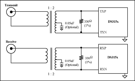
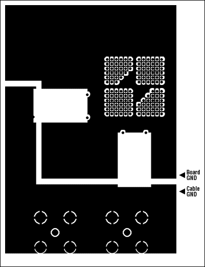
Figure 1-5. DS3151 Single-port, T3/E3 LIU ground plane {layer two} layout—no ground plane under the transformers.
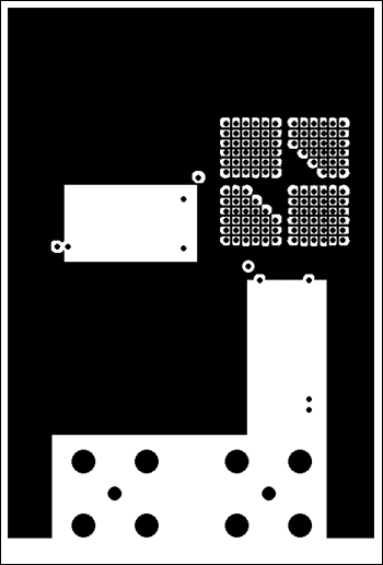
Figure 1-6. DS3151 Single-port, T3/E3 LIU VCC plane {layer three} layout—no VCC plane under the transformer or TXP, TXN, RXP, RXN.
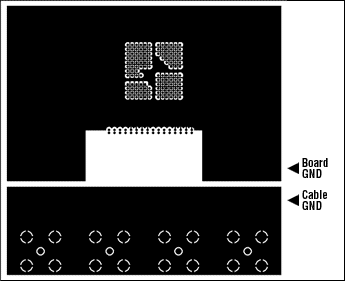
Figure 2-5. DS3152 dual-port, T3/E3 LIU ground plane {layer two} layout—no ground plane under the transformer.
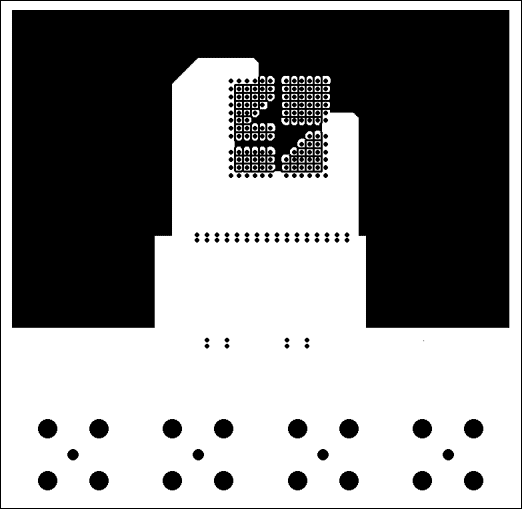
Figure 2-6. DS3152 dual-port, T3/E3 LIU VCC plane {layer three} layout—no VCC plane under the transformer or TXP, TXN, RXP, RXN.
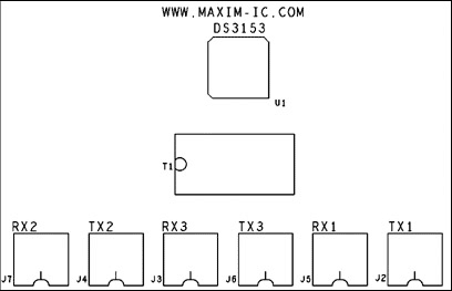
Figure 3-1. DS3153 triple-port, T3/E3 LIU layout—silkscreen top layer.
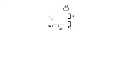
Figure 3-2. DS3153 triple-port, T3/E3 LIU layout—silkscreen bottom layer (view mirrored).
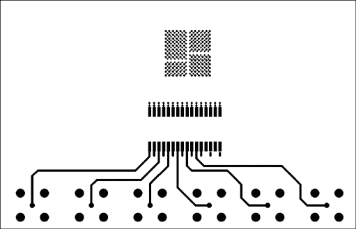
Figure 3-3. DS3153 triple-port, T3/E3 LIU layout—top conducting layer.
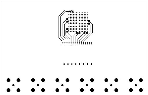
Figure 3-4. DS3153 triple-port, T3/E3 LIU layout—bottom conducting layer.
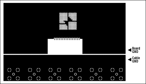
Figure 3-5. DS3153 triple-port, T3/E3 LIU ground plane {layer two} layout—no ground plane under the transformer.
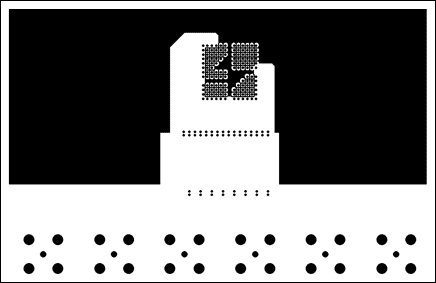
Figure 3-6. DS3153 triple-port, T3/E3 LIU VCC plane {layer three} layout—no VCC plane under the transformer or TXP, TXN, RXP, RXN.
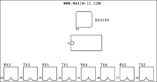
Figure 4-1. DS3154 quad-port, T3/E3 LIU layout—silkscreen top layer.
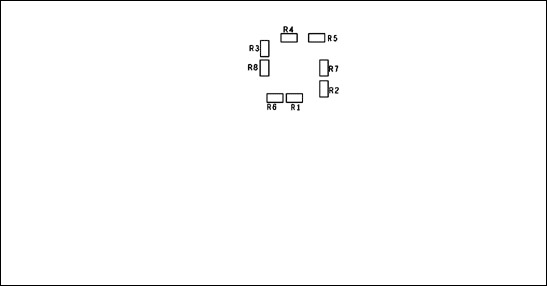
Figure 4-2. DS3154 quad-port, T3/E3 LIU silkscreen layout—bottom layer (view mirrored).
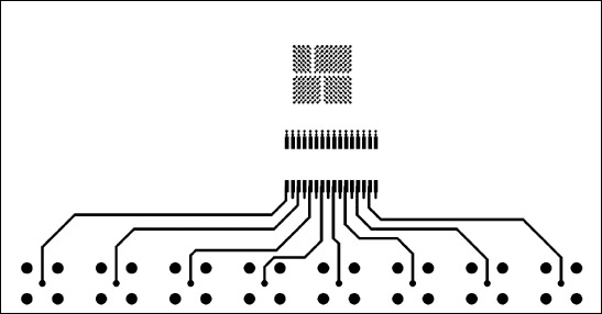
Figure 4-3. DS3154 quad-port, T3/E3 LIU layout—top conducting layer.
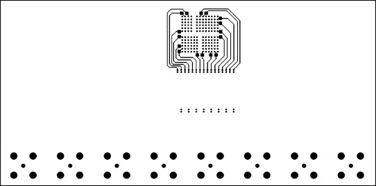
Figure 4-4. DS3154 quad-port, T3/E3 LIU layout—bottom conducting layer.
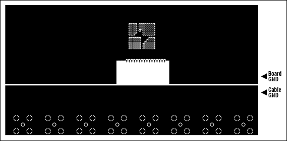
Figure 4-5. DS3154 quad-port, T3/E3 LIU ground plane {layer two} layout—no ground plane under the transformer.
Figure 4-6. DS3154 quad-port, T3/E3 LIU VCC plane {layer three} layout—no VCC plane under the transformer or TXP, TXN, RXP, RXN.
If you have further questions about our T3/E3 products, please contact the Telecommunication Applications support team by email, telecom.support@dalsemi
打开APP阅读更多精彩内容
Overview
This application note is a guideline on how to layout the network interface for Dallas Semiconductor T3/E3 line interface units (LIUs). The guideline uses the DS315x products as examples. This application note is also applicable for other Dallas Semiconductor T3/E3 products.The DS315x products include the DS3151 (single), DS3152 (dual), DS3153 (triple), and DS3154 (quad) LIUs which perform the necessary functions for interfacing at the physical layer to a DS3, E3, or STS-1 line. Each LIU has independent receive and transmit paths.
Each layout shows the communication line routing between the DS315x LIU, the transformer, and the 75Ω BNC connectors. In particular, each layout defines the recommended trace widths to ensure the proper impedance for a given network interface. All board stack-ups are the same.
Board Stackup
Below is an example of the trace-width calculation for a T3/E3 LIU interface.
| Surface Materials |
Thickness | Dielectric Constant |
Line Widths |
Impedance | |
| TX, RX @ 75Ω | |||||
 |
Top conductor copper | 1.2MIL | N/A | 25MIL | 75Ω |
| Dielectric FR-4 | 21.57MIL | 4.5 | N/A | N/A | |
| L2_GND conductor copper | 0.7MIL | N/A | N/A | N/A | |
| TXP, TXN, RXP, RXN @ 150Ω | |||||
| Bottom conductor copper | 1.2MIL | N/A | 5MIL | 150Ω | |
| Dielectric FR-4 | 61.53MIL | 4.5 | N/A | N/A | |
| L2_GND conductor copper | 0.7MIL | N/A | N/A | N/A | |
Basic Network Interface
Layout Considerations
- Impedance
- Location—keep termination resistors as close to the LIU as possible.
- Trace widths—keep trace widths as short as possible.
- Do not route the GND plane under the transformer to reduce noise.
- Do not route the VCC plane under the transformer or TXP, TXN, RXP, RXN routes.
- Isolate the GND plane between board and cable.
Layout Examples
Example 1: DS3151—The layout of a single-port T3/E3 LIU
Table 1-1. Layout Components| Name | Qty | Description | Supplier | Part Number |
| U1 | 1 | Single DS3/E3/STS1 LIU, 144P BGA | Dallas Semiconductor | DS3151 |
| C1,C2 | 2 | 0805 Ceram 56000pF, 25V 10% | Panasonic | ECJ-2VB1E563K |
| R1,R2 | 2 | Resistor, 0603 332Ω, 1/16W 1% | Panasonic | ERJ-3EKF3320V |
| T1,T2 | 2 | Transformer, 1:2 T3/E3/STS-1, industrial | Pulse | T3012 |
| J1,J2 | 2 | Connector, BNC 75Ω, RA 5-pin | Trompetor | UCBJR220 |
 Figure 1-1. DS3151 Single-port, T3/E3 LIU layout—silkscreen top layer. |
 Figure 1-2. DS3151 Single-port ,T3/E3 LIU layout—silkscreen bottom layer (view mirrored). |
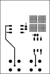 Figure 1-3. DS3151 Single-port, T3/E3 LIU layout—top conducting layer. |
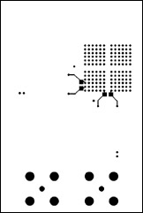 Figure 1-4. DS3151 Single-port, T3/E3 LIU layout—bottom conducting layer. |
Figure 1-5. DS3151 Single-port, T3/E3 LIU ground plane {layer two} layout—no ground plane under the transformers.
Figure 1-6. DS3151 Single-port, T3/E3 LIU VCC plane {layer three} layout—no VCC plane under the transformer or TXP, TXN, RXP, RXN.
Example 2: DS3152—The Layout of a Dual-Port T3/E3 LIU
Table 2-1. Layout Components| Name | Qty | Description | Supplier | Part Number |
| U1 | 1 | Dual DS3/E3/STS1 LIU, 144P BGA | Dallas Semiconductor | DS3152 |
| R1-R4 | 4 | Resistor, 0603 332Ω, 1/16W 1% | Panasonic | ERJ-3EKF3320V |
| T1 | 1 | Transformer, OCTAL T3/E3, 1:2, SMT 32-pin | Pulse | T3049 |
| J2,J4,J5,J7 | 4 | Connector, BNC 75Ω, RA 5-pin | Trompetor | UCBJR220 |
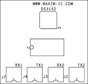 Figure 2-1. DS3152 dual-port, T3/E3 LIU layout— silkscreen top layer. |
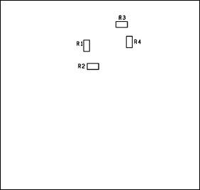 Figure 2-2. DS3152 dual-port,T3/E3 LIU layout— silkscreen bottom layer (view mirrored). |
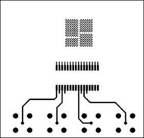 Figure 2-3. DS3152 Dual-port, T3/E3 LIU layout—top conducting layer. |
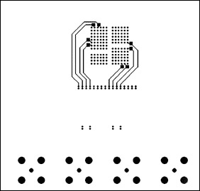 Figure 2-4. DS3152 dual-port, T3/E3 LIU layout—bottom conducting layer. |
Figure 2-5. DS3152 dual-port, T3/E3 LIU ground plane {layer two} layout—no ground plane under the transformer.
Figure 2-6. DS3152 dual-port, T3/E3 LIU VCC plane {layer three} layout—no VCC plane under the transformer or TXP, TXN, RXP, RXN.
Example 3: DS3153—The Layout of a Triple-Port, T3/E3 LIU
Table 3-1. Layout Components| Name | Qty | Description | Supplier | Part Number |
| U1 | 1 | Triple DS3/E3/STS1 LIU, 144P BGA | Dallas Semiconductor | DS3153 |
| R1-R5,R7 | 6 | Resistor, 0603 332Ω, 1/16W 1% | Panasonic | ERJ-3EKF3320V |
| T1 | 1 | Transformer, OCTAL T3/E3, 1:2, SMT 32-pin | Pulse | T3049 |
| J2-J7 | 6 | Connector, BNC 75Ω, RA 5-pin | Trompetor | UCBJR220 |
Figure 3-1. DS3153 triple-port, T3/E3 LIU layout—silkscreen top layer.
Figure 3-2. DS3153 triple-port, T3/E3 LIU layout—silkscreen bottom layer (view mirrored).
Figure 3-3. DS3153 triple-port, T3/E3 LIU layout—top conducting layer.
Figure 3-4. DS3153 triple-port, T3/E3 LIU layout—bottom conducting layer.
Figure 3-5. DS3153 triple-port, T3/E3 LIU ground plane {layer two} layout—no ground plane under the transformer.
Figure 3-6. DS3153 triple-port, T3/E3 LIU VCC plane {layer three} layout—no VCC plane under the transformer or TXP, TXN, RXP, RXN.
Example 4: DS3154—The Layout of a Quad-Port, T3/E3 LIU
Table 4-1. Layout Components| Name | Qty | Description | Supplier | Part Number |
| U1 | 1 | Quad DS3/E3/STS1 LIU, 144P BGA | Dallas Semiconductor | DS3154 |
| R1-R8 | 8 | Resistor, 0603 332Ω, 1/16W 1% | Panasonic | ERJ-3EKF3320V |
| T1 | 1 | Transformer, OCTAL T3/E3, 1:2, SMT 32-pin | Pulse | T3049 |
| J1-J8 | 8 | Connector, BNC 75Ω, RA -pin | Trompetor | UCBJR220 |
Figure 4-1. DS3154 quad-port, T3/E3 LIU layout—silkscreen top layer.
Figure 4-2. DS3154 quad-port, T3/E3 LIU silkscreen layout—bottom layer (view mirrored).
Figure 4-3. DS3154 quad-port, T3/E3 LIU layout—top conducting layer.
Figure 4-4. DS3154 quad-port, T3/E3 LIU layout—bottom conducting layer.
Figure 4-5. DS3154 quad-port, T3/E3 LIU ground plane {layer two} layout—no ground plane under the transformer.
Figure 4-6. DS3154 quad-port, T3/E3 LIU VCC plane {layer three} layout—no VCC plane under the transformer or TXP, TXN, RXP, RXN.
Conclusion
This application note illustrated what is necessary to maintain the proper impedance for a T3/E3 networking interface using the DS315x.If you have further questions about our T3/E3 products, please contact the Telecommunication Applications support team by email, telecom.support@dalsemi
Cadence is a registered trademark of Cadence Design Systems, Inc.
声明:本文内容及配图由入驻作者撰写或者入驻合作网站授权转载。文章观点仅代表作者本人,不代表电子发烧友网立场。文章及其配图仅供工程师学习之用,如有内容侵权或者其他违规问题,请联系本站处理。
举报投诉
- 相关推荐
- 热点推荐
- Interfaces
-
全志t3和a40i有什么区别?2023-08-16 7160
-
T3/A40i支持Linux-5.10新内核啦,Docker、Qt、Python统统升级!2023-07-31 2225
-
请查收“国产化率认证报告”(100%)——T3/A40i工业核心板2023-02-13 10992
-
全志T3(A40I)/T5(T507)性能对比,一代更比一代强2022-05-27 12117
-
T3/A40i全国产方案参数详解!2022-01-24 4920
-
锤子T3什么时候上市?锤子T3最新消息:锤子T3又有新消息了一好一坏,罗永浩的锤子T3有惊喜?2017-07-03 33544
-
锤子T3什么时候上市?锤子T3最新消息:锤子T3设计、配置、性能要搞事情,锤子T3或到明年依然值得期待2017-06-27 5295
-
锤子T3最新消息:听说T系列没了?罗永浩说:坚果Pro其实就是原来的锤子T32017-05-10 21100
-
春天都要过去了!锤子T3/T3X什么时候发布?2017-04-06 2178
-
锤子T3:只闻其声未见其身?锤子T3渲染图曝光,双摄+双曲面!惊艳2017-03-29 2576
-
锤子T3曝光:简直美哭了2016-08-15 5666
-
T3(E3)保护电路及解决方案2009-11-20 2297
-
T3/E3/STS-1光纤扩展-T3/E3/STS-1 Fi2009-04-29 1240
-
HFTA-09.0: T3/E3/STS-1 Fiber O2009-04-20 1528
全部0条评论

快来发表一下你的评论吧 !
