
HFTA-09.0: T3/E3/STS-1 Fiber O
通信设计应用
描述
Introduction
Typically, T3/E3/STS-1 signals are run over short distances, but some applications require a much longer distance. A T3/E3/STS-1 fiber-to-copper converter takes the copper signal and converts it to an optical signal to be transported over a fiber link. A pair of converters extends the T3/E3/STS-1 signal beyond the copper specification, allowing the T3/E3/STS-1 signal to be used beyond the intrabuilding length limitation. While the standard length for a T3 signal is 380m, an E3 signal length is 440m, and an STS-1 standard signal length is 360m, a fiber connection can reach miles. However, no standard exists for transporting T3/E3/STS-1 over fiber. Typical designs can include single-mode or multi-mode fiber using SC or ST connectors, and different optical wavelengths, such as 850nm, 1310nm, and 1550nm. The optic budget length determines if the engineer needs to enhance the optical component design to satisfy the end user's application.To transmit data via fiber optic cables, the signals must first be converted from the electrical domain to the optical domain. At the receiver, the process is reversed. Most designs use two fiber strands for each direction: Tx and Rx. However, because of the unique properties of light, an optical diplexer can be used so that a full-duplex connection can be designed over one strand of fiber, using the same wavelength for both directions. This application note discusses a simple, full-duplex system using two strands of single-mode fiber for longer distances.
The STS-1 is the basic unit of transmission in the Synchronous Optical Network (SONET). It is the copper-based version of OC-1. STS-1 is also known as EC-1. Both T3 and E3 are at the third hierarchy within the Plesiochronous Digital Hierarchy (PDH). Table 1 illustrates the respective bit rates.
Table 1. Bit Rates vs. Hierarchical Standards
| Bit Rate | Hierarchy |
| 34.368Mbps (E3) |
PDH |
| 44.736Mbps (T3) |
PDH |
| 51.840Mbps (STS-1) |
SONET |
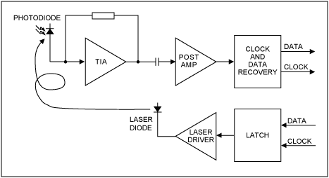
In a time-division multiplex (TDM) system, the Manchester technique is typically used for the line encoding/decoding of the clock and data together. As for modulation of the optical signal on the fiber, the laser/LED transmitter/receiver uses the "light on" for a binary 1, and "light off" for a binary 0. As optical receivers detect signals from the fiber and convert them back to electrical signals, they must be amplified before the clock and data can be recovered. Figure 1 shows a block diagram of a typical receiver and transmitter pair for an optical TDM system.

Figure 1. A typical receiver/transmitter pair for oOptical TDM transmission.
Optical Receiver Performance
At the receiving end of the optical link, a PIN diode or Avalanche Photodiode (APD) photodetector converts the received light to a current signal. The PIN diode operates at the same supply of the other components of 3.3V and is relatively cheaper than the APD. However, for a given optical power received, the PIN diode emits fewer electrons than the APD, so the APD is the better choice if the receiver needs to be placed further away from the transmitter. Unlike the PIN diode, the APD needs a biasing circuit, which may require a reverse operating voltage in the 30V to 100V range. In addition to the increased cost, the APD adds more noise to the circuit and requires cooling.The photodetector delivers the output current to a transimpedance amplifier (TIA). The TIA converts this current to a voltage, amplifies this single-ended voltage, then converts it to a differential signal. The TIA should provide both a large dynamic range and high overload tolerance on the input. TIA noise must be reduced to provide the high input sensitivity necessary to receive optical signals weakened by transmitter aging and/or long transmission distance. A high overload tolerance is required to avoid bit errors due to distortion in the presence of strong optical signals. The TIA's maximum gain depends on its operating frequency, which should be optimized only within a narrow range, to ensure stable operation. The TIA function must be followed by a postamplifier, commonly known as a limiting amplifier (LA). The LA delivers an output-voltage swing whose maximum is independent of the input signal strength.
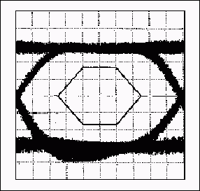
The clock and data recovery (CDR) block follows the LA. The CDR regenerates the original clock and data stream by performing timing and amplitude-level decisions on the incoming signal from the LA. The challenge for an integrated clock-recovery circuit is to meet the jitter specification recommendations. When several pseudo-random bit-pattern sequences are superimposed, the signal quality can be seen in an "eye diagram" (see Figure 2).

Figure 2. An "Eye Diagram" illustrates the quality of a data stream.
Because the CDR must accept a certain amount of input data jitter to achieve normal error-free operation, all receiver units in line-termination and regenerator applications must comply with recommendations for jitter tolerance. Jitter transfer refers to the portion of jitter allowed to transfer from input to output of the CDR, and jitter generation is that produced by the CDR itself. At each stage in the system, the recovered clock enables transmission to the next regenerator, allowing jitter contributions to accumulate. Line-termination receivers do not need to meet jitter transfer and jitter generation specifications because the regenerated data is synchronized to the system clock.
For data recovery it is important to use a phase-locked loop (PLL) to synchronize the clock with the data stream, which will ensure alignment of the clock with the middle of a data word. The optical receiver system should include the option to adjust the phase relation between the clock and data. This will help minimize the bit-error rate (BER) in the presence of asymmetrical rise and fall transitions of the received data signal.
Optical Transmitter Performance
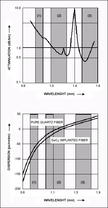
At the transmitting end of the optical link, a laser diode or LED coverts the electrical bit sequence to pulses of light. The second and third optical windows are typically used for transmitting information over standard fiber cable in telecommunication networks, as shown in Figure 3. Inside an optical window, the signals benefit from less dispersion and less attenuation per unit of fiber length. The laser diode or LED is modulated by the "laser driver" block (see Figure 1).
Figure 3. Attenuation and dispersion of first, second, and third optical windows.
The direct modulated semiconductor laser diode, such as the electro-absorption, distributed feedback, and Mach-Zehnder types, is an optical source with high spectral purity that can operate in the third optical window. Thus, the laser diode is preferred for very long distance and/or very high bit rates. All semiconductor laser diodes used for direct modulation need a DC bias current to set the operating point and a modulation current for signal transmission. The values for DC bias and modulation current depend on characteristics of the laser diode, which can differ from type to type.
To compensate for the drift of laser characteristics over time and temperature, the laser driver must maintain the initially adjusted DC operating point. To compensate, an automatic-power control (APC) is usually integrated within the laser driver. To detect the actual laser power output, an internal monitoring photodiode converts the laser light to a proportional current and feeds it back to the laser driver for comparison with the output set point. Any difference causes the DC bias current to increase or decrease as required to reach the original set point.
It may also be necessary to compensate for a change in the optical signal strength caused by time and temperature. This is solved either with additional external circuitry or with an integrated automatic-modulation control (AMC). The AMC typically uses the monitor photodiode already present in the APC loop. In addition to these functions, the system must be capable of stopping laser transmissions by disabling the driver without interrupting data reception at the input.
Specific System Blocks
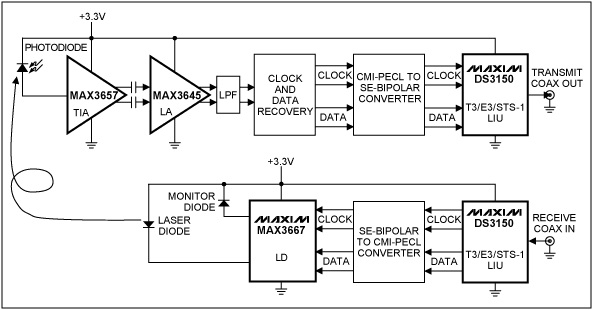
The following section describes a complete system that optimizes the above criteria and uses Maxim/Dallas parts where available. Figure 4 shows a signal chain of an optical transceiver for T3/E3/STS-1 operation. In the optical receiver side, the MAX3657 was selected as the TIA where the AC coupling of the outputs are large to minimize wander. The MAX3645 is the LA and contains a loss-of-signal detector. The low-pass filter required after the LA needs to be a fourth-order Bessel or linear-phase LPF, where the 3dB bandwidth set point is selected as 80% of the selected bit rate. The CDR device needs to use Manchester decoding and output either code-mark inversion/positive emitter-coupled logic (CMI/PECL) differential signals or single-ended clock and data. The CMI/PECL differential to single-ended bipolar clock and data converter block may be necessary to condition the signals for the DS3150 LIU to transmit out the coaxial line.In the optical transmitter side, the MAX3667 with APC was selected as the LD. A single-ended bipolar to CMI/PECL differential converter is also needed to take the clock and data stream from the DS3150 LIU that is received from the coaxial line. The system in Figure 4 shows only one side of a T3/E3/STS-1 transceiver. Another set would be required to allow for full-duplex operation. Please see the respective data sheets for specific design procedures. If an APD is used instead of the PIN diode for the photodiode, then the MAX1932 can provide its bias and can be controlled by the MAX1968.

Figure 4. A transceiver system for optical TDM transmission using Maxim and Dallas parts.
T3/E3/STS-1 Fiber Optic Extension Information
For further questions on T3/E3/STS-1 Fiber Optic Extension, please contact the Telecommunication Applications support team via email at telecom.support@dalsemi.com, or call 972-371-6555.For more information about the DS3150, please consult the DS3150 data sheet available on our website at www.maxim-ic.com/telecom.
For more information about the MAX3657, MAX3645, MAX3667, MAX1932, or MAX1968, please consult the data sheets available on at www.maxim-ic.com/fiber.
-
HFTA-09.0: T3/E3/STS-1光纤扩展2023-06-10 1865
-
HFTA-09.0: T3/E3/STS-1 光纤扩展2023-03-03 1846
-
T3和E3网络接口布局指南2023-02-22 3828
-
T3/E3/STS-1 LIU二次浪涌保护设计2023-02-13 2057
-
T3/E3/STS-1光纤扩展知识点总结的太棒了2021-05-31 2154
-
DS3 / E3 / STS成帧器设计用于多标准网络和传输系统2019-09-03 1883
-
T3(E3)保护电路及解决方案2009-11-20 2276
-
T3/E3/STS-1光纤扩展-T3/E3/STS-1 Fi2009-04-29 1213
-
DS31256 Unchannelized T3/E3/HS2009-04-20 1367
-
DS317x与DS318x T3/E3/STS-1 LIU回2009-04-18 1168
-
DS3150 业内首款单端口T3/E3 LIU,集成了抖动衰2008-09-19 1732
全部0条评论

快来发表一下你的评论吧 !

