
Using DS2148/348 as Repeater
通信设计应用
65人已加入
描述
Abstract: Application Note 387 describes the use of the Dallas Semiconductor/Maxim DS2148/DS21348 as a T1 or E1 repeater. A simple circuit diagram shows typical connections. Configurations for Hardware Mode and Software Mode are also provided.
The receive sensitivity for these two LIUs is programmable and is as much as -36dB for T1 applications and -43dB for E1 applications.
To simplify the design, it is recommended to use a 2.048MHz oscillator and use the internal register settings of the DS2148 and the DS21348 to convert the MCLK to 1.544MHz for T1 applications.

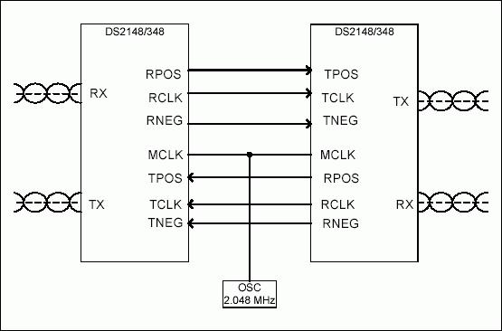
Figure 1. Typical T1/E1 repeater application.
The configuration settings of the DS2148 or the DS21348 in hardware mode are:
The configuration settings of the DS2148 or the DS21348 in software mode are:
打开APP阅读更多精彩内容
Introduction
This application note describes the register settings for Dallas Semiconductor's DS2148 and DS21348 (E1/T1/J1 line interface units) as a repeater for T1 or E1 operation. This can be accomplished with the device in either hardware or software mode.The receive sensitivity for these two LIUs is programmable and is as much as -36dB for T1 applications and -43dB for E1 applications.
To simplify the design, it is recommended to use a 2.048MHz oscillator and use the internal register settings of the DS2148 and the DS21348 to convert the MCLK to 1.544MHz for T1 applications.

Figure 1. Typical T1/E1 repeater application.
The configuration settings of the DS2148 or the DS21348 in hardware mode are:
| HARDWARE MODE SETTINGS FOR T1 | HARDWARE MODE SETTINGS FOR E1 |
| MCLK = 2.048MHz | MCLK = 2.048MHz |
| BIS1 = 1, BIS0 = 1 | BIS1 = 1, BIS0 = 1 |
| CES = 0 | CES = 0 |
| DJA = 0 or 1 (application dependent) | DJA = 0 or 1 (application dependent) |
| HBE = 1 | HBE = 1 |
| JAS = 0 or 1 (application dependent) | JAS = 0 or 1 (application dependent) |
| NRZE = 0 | NRZE = 0 |
| TPD = 0 | TPD = 0 |
| L2 = L1 = L0 = 0 | L2/L1/L0 (application dependent) |
| TX1 = 0, TX0 = 0 | TX1 = 0, TX0 = 0 |
| LOOP1 = 0, LOOP0 = 0 | LOOP1 = 0, LOOP0 = 0 |
| EGL = 1, ETS = 1 (limited long haul) EGL = 0, ETS = 1 (long haul) |
EGL = 0, ETS = 0 (short haul) EGL = 1, ETS = 0 (long haul) |
| MM1 = 0, MM0 = 0 | MM1 = 0, MM0 = 0 |
| RT1 = 1, RT0 = 0 (internal Rx side, 100Ω enabled) | RT1 = 0, RT0 = 1 (internal Rx side, 120Ω enabled) RT1 = 1, RT0 = 1 (internal Rx side, 75Ω enabled) |
| JAMUX = 1, ETS = 1 | JAMUX = 1, ETS = 0 |
The configuration settings of the DS2148 or the DS21348 in software mode are:
| SOFTWARE MODE REGISTER SETTINGS FOR T1 | SOFTWARE MODE REGISTER SETTINGS FOR E1 | ||
| MCLK = 2.048MHz | MCLK = 2.048MHz | ||
| CCR1 (00H) | CCR1.7 = 1 CCR1.6 = 0 CCR1.3 = 1 CCR1.1 = 1 |
CCR1 (00H) | CCR1.7 = 0 CCR1.6 = 0 CCR1.3 = 1 CCR1.1 = 1 |
| CCR2 (01H) | CCR2.3 = 1 CCR2.2 = 1 CCR2.1 = 0 CCR2.0 = 0 |
CCR2 (01H) | CCR2.3 = 1 CCR2.2 = 1 CCR2.1 = 0 CCR2.0 = 0 |
| CCR4 (03H) | CCR4.7 = CCR4.6 = CCR4.5 = 0 CCR4.1 (application dependent) CCR4.0 = 0 |
CCR4 (03H) | CCR4.7, CCR4.6, and CCR4.5 (application dependent) CCR4.1 (application dependent) CCR4.0 = 0 |
| CCR5 (04H) | CCR5.5 = 0, CCR5.4 = 0 CCR5.1 = 1, CCR5.0 = 0 (internal Rx side, 100Ω enabled) |
CCR5 (04H) | CCR5.5 = 0, CCR5.4 = 0 CCR5.1 = 0, CCR5.0 = 1 (internal RX side, 120Ω enabled) CCR5.1 = 1, CCR5.0 = 1 (internal Rx side, 75Ω enabled) |
声明:本文内容及配图由入驻作者撰写或者入驻合作网站授权转载。文章观点仅代表作者本人,不代表电子发烧友网立场。文章及其配图仅供工程师学习之用,如有内容侵权或者其他违规问题,请联系本站处理。
举报投诉
- 相关推荐
- 热点推荐
- Using
-
DS2148、DS21348、DS21Q48、DS21Q348和DS21448的附加脉冲幅度设置2023-02-13 2553
-
DS2148G 接口 - 电信2023-01-30 109
-
DS2148T+ 接口 - 电信2023-01-14 100
-
什么是中继器(Repeater)2010-04-03 2233
-
DS2148/DS21348 Hardware Mode2009-04-20 1751
-
Using the DS32kHz with Dallas2009-03-31 848
全部0条评论

快来发表一下你的评论吧 !

