


D4 Framing and Signaling
通信设计应用
65人已加入
描述
Abstract: Application note 310 contains information necessary to control D4 framing and signaling on the Dallas Semiconductor T1 devices. It incorporates the necessary information to enable both transmit and receive D4 framing and signaling. For the transmit path, programming of the registers for framing and signaling operations are discussed in detail. For the receive path, programming of the registers for recovering framing and signaling is discussed along with receive interrupt handling. The application note provides all the necessary information to get the Dallas Semiconductor T1 device operating in D4 mode.
All Dallas Semiconductor T1 framers and single-chip transceivers (SCTs) provide support for D4 framing and signaling, as shown in Figure 1. This application note provides the requirements to enable the D4 format in the transmit and receive paths for T1 framers and SCTs.
For the transmit path, programming the registers for framing and signaling operations are discussed. For the receive path, programming the registers to retrieve framing and signaling is discussed along with receive interrupt handling.
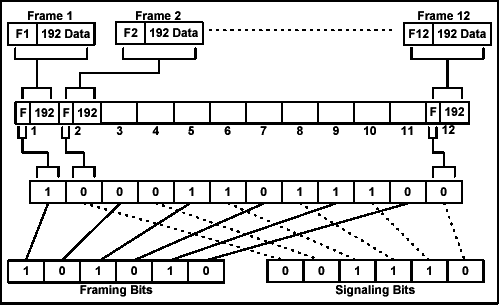
Figure 1. D4 framing format.
Table 1. D4 Framing Register Settings
Table 2. Transmit Signaling Registers
Table 3. Transmit Signaling Register Map (D4 Format)
Table 4. Receive Signaling Registers (D4 Format)
If you have further questions concerning the operation of our T1 framers or SCTs, please contact the Telecommunication Applications support team via email at telecom.support@dalsemi.com or call 972-371-6555.
打开APP阅读更多精彩内容
Introduction
This application note applies to the following products:| T1 Framers | T1 SCTs |
| DS2141A | DS2151 |
| DS21Q41B | DS2152 |
| DS21Q42 | DS21352 |
| DS21FF42 | DS21552 |
| DS21FT42 | DS21Q352 |
| DS21Q352 |
All Dallas Semiconductor T1 framers and single-chip transceivers (SCTs) provide support for D4 framing and signaling, as shown in Figure 1. This application note provides the requirements to enable the D4 format in the transmit and receive paths for T1 framers and SCTs.
For the transmit path, programming the registers for framing and signaling operations are discussed. For the receive path, programming the registers to retrieve framing and signaling is discussed along with receive interrupt handling.
Figure 1. D4 framing format.
D4 Framing Register Settings
Several registers must be initialized to enable D4 multiframing. Table 1 shows the register settings required to generate and receive D4 multiframing.Table 1. D4 Framing Register Settings
| Register Setting | Function |
| CCR2.7, CCR2.3 = 0 | Selects D4 multiframing in the transmit and receive directions. |
| CCR2.5 = 1 | Enables insertion of the 6-bit Fs pattern. |
| TFDL = 1Ch | This is the 6-bit Fs pattern. |
| RCR1.3 = 1 | If this bit is cleared, the receiver declares synchronization on the Ft pattern only and will not be guaranteed to find the D4 multiframe boundary. |
| Toggle low to high RCR1.0 | Required after configuring the control registers to force resynchronization. |
Transmit Signaling Registers
In D4 multiframing, only six of the 12 transmit signaling registers are needed to load a multiframe of signaling. The transmitter alternates, loading the contents of TS1 through TS6 into one multiframe, followed by the contents of TS7 through TS12 into the next multiframe, then back again. Therefore, load the transmit signaling bytes into two registers, as shown in Table 2. A full register map shows the bits of each transmit signaling register in Table 3.Table 2. Transmit Signaling Registers
| Register | Description |
| TS1 and TS7 | A bits for channels 1 through 8 |
| TS2 and TS8 | A bits for channels 9 through 16 |
| TS3 and TS9 | A bits for channels 17 through 24 |
| TS4 and TS10 | B bits for channels 1 through 8 |
| TS5 and TS11 | B bits for channels 9 through 16 |
| TS6 and TS12 | B bits for channels 17 through 24 |
Table 3. Transmit Signaling Register Map (D4 Format)
| (MSB) | (LSB) | |||||||
| TS1 (70h) | CH8-A | CH7-A | CH6-A | CH5-A | CH4-A | CH3-A | CH2-A | CH1-A |
| TS2 (71h) | CH16-A | CH15-A | CH14-A | CH13-A | CH12-A | CH11-A | CH10-A | CH9-A |
| TS3 (72h) | CH24-A | CH23-A | CH22-A | CH21-A | CH20-A | CH19-A | CH18-A | CH17-A |
| TS4 (73h) | CH8-B | CH7-B | CH6-B | CH5-B | CH4-B | CH3-B | CH2-B | CH1-B |
| TS5 (74h) | CH16-B | CH15-B | CH14-B | CH13-B | CH12-B | CH11-B | CH10-B | CH9-B |
| TS6 (75h) | CH24-B | CH23-B | CH22-B | CH21-B | CH20-B | CH19-B | CH18-B | CH17-B |
| TS7 (76h) | CH8-A | CH7-A | CH6-A | CH5-A | CH4-A | CH3-A | CH2-A | CH1-A |
| TS8 (77h) | CH16-A | CH15-A | CH14-A | CH13-A | CH12-A | CH11-A | CH10-A | CH9-A |
| TS9 (78h) | CH24-A | CH23-A | CH22-A | CH21-A | CH20-A | CH19-A | CH18-A | CH17-A |
| TS10 (79h) | CH8-B | CH7-B | CH6-B | CH5-B | CH4-B | CH3-B | CH2-B | CH1-B |
| TS11(7Ah) | CH16-B | CH15-B | CH14-B | CH13-B | CH12-B | CH11-B | CH10-B | CH9-B |
| TS12(7Bh) | CH24-B | CH23-B | CH22-B | CH21-B | CH20-B | CH19-B | CH18-B | CH17-B |
Receive Signaling Registers
Table 4 provides a detailed view of the bits of each receive signaling register. Signaling from the most recent multiframe is loaded into RS7 through RS12. Signaling from the previous multiframe is moved from RS7 through RS12 and copied to RS1 through RS6. Older signaling is discarded.Table 4. Receive Signaling Registers (D4 Format)
| (MSB) | (LSB) | |||||||
| RS1 (60h) | CH8-A | CH7-A | CH6-A | CH5-A | CH4-A | CH3-A | CH2-A | CH1-A |
| RS2 (61h) | CH16-A | CH15-A | CH14-A | CH13-A | CH12-A | CH11-A | CH10-A | CH9-A |
| RS3 (62h) | CH24-A | CH23-A | CH22-A | CH21-A | CH20-A | CH19-A | CH18-A | CH17-A |
| RS4 (63h) | CH8-B | CH7-B | CH6-B | CH5-B | CH4-B | CH3-B | CH2-B | CH1-B |
| RS5 (64h) | CH16-B | CH15-B | CH14-B | CH13-B | CH12-B | CH11-B | CH10-B | CH9-B |
| RS6 (65h) | CH24-B | CH23-B | CH22-B | CH21-B | CH20-B | CH19-B | CH18-B | CH17-B |
| RS7 (66h) | CH8-A | CH7-A | CH6-A | CH5-A | CH4-A | CH3-A | CH2-A | CH1-A |
| RS8 (67h) | CH16-A | CH15-A | CH14-A | CH13-A | CH12-A | CH11-A | CH10-A | CH9-A |
| RS9 (68h) | CH24-A | CH23-A | CH22-A | CH21-A | CH20-A | CH19-A | CH18-A | CH17-A |
| RS10 (69h) | CH8-B | CH7-B | CH6-B | CH5-B | CH4-B | CH3-B | CH2-B | CH1-B |
| RS11(6Ah) | CH16-B | CH15-B | CH14-B | CH13-B | CH12-B | CH11-B | CH10-B | CH9-B |
| RS12(6Bh) | CH24-B | CH23-B | CH22-B | CH21-B | CH20-B | CH19-B | CH18-B | CH17-B |
Receive Interrupt Handling
Two interrupts can be used to give the user notification that the receive signaling registers need to be retrieved:- Receive Multiframe Interrupt (RMF):
- The RMF bit in Status Register 2 (SR2.7) is set and the bits in the receive signaling registers are updated on receive multiframe boundaries. Therefore, the RMF interrupt can be used to determine when to retrieve the receive signaling registers. Setting bit 7 of the Interrupt Mask Register 2 (IMR2.7) enables the RMF interrupt.
- Receive Signaling Change Interrupt (RSC):
- The RSC bit in Status Register 2 (SR2.0) is set when a change of sate is detected in any of the signaling bits. Setting bit 0 of the Interrupt Mask Register 2 (IMR2.0) enables the RSC interrupt. Once a signaling change has been detected, the user has at least 2.75ms to read the data before it is lost.
D4 Framing and Signaling Information
For more information about Dallas Semiconductor's T1 framers and SCTs, please consult the data sheets available on our website at www.maxim-ic.com/telecom.If you have further questions concerning the operation of our T1 framers or SCTs, please contact the Telecommunication Applications support team via email at telecom.support@dalsemi.com or call 972-371-6555.
声明:本文内容及配图由入驻作者撰写或者入驻合作网站授权转载。文章观点仅代表作者本人,不代表电子发烧友网立场。文章及其配图仅供工程师学习之用,如有内容侵权或者其他违规问题,请联系本站处理。
举报投诉
- 相关推荐
- 热点推荐
- Signaling
-
AFE4400评估板里面的BAV99W-7-F(D1、D2、D3、D4)是不是可以去掉?2024-12-30 248
-
5G新开站点D4频段干扰案例分享2023-12-12 3291
-
NodeMCU只有引脚D4与onewire ds18b20一起工作吗?2023-04-28 383
-
ESP32 PICO D4引导加载程序重置是怎么回事?2023-04-12 711
-
如何在Wemos D1 mini D4引脚上运行中断?2023-02-27 412
-
ESP32 PICO D4技术规格书2022-09-23 1075
-
分析C2\C3\D3\D4作用,C1上为什么会有500V电压2020-04-26 2056
-
英特尔实感D4视觉处理器可作为协处理器吗?2018-11-14 3990
-
请问AD5933状态寄存器位D0和位D4至D7是无关位吗?2018-10-11 3101
-
stc单片机PCON寄存器的D6,D5,D4位怎么用?2014-10-09 3161
-
CES2012:尼康新品单反D4现场把玩2012-01-12 1772
-
DS2141A, DS2151 D4 Framing App2009-04-20 941
全部0条评论

快来发表一下你的评论吧 !
