

DS21352/552, DS2151, DS2152, D
通信设计应用
65人已加入
描述
Abstract: This application note describes how to use the SLC-96 mode found in all Dallas Semiconductor T1 framers and single chip transceivers (SCTs). The SLC-96 mode is used in T1 was designed by AT&T as a digital loop carrier system that provides service for 96 subscribers over 3 to 5 separate T1 lines. The frame format of SLC-96 closely resembles that of the super frame (SF or D4) format but additional data link information is transferred to make advanced functions such as single party, multiparty, coin telephone, and special service circuits available. Because of the complexity of the SLC-96 specification, special synchronization circuitry, data registers, and status registers were added to the T1 devices which allow the designer to take advantage of the SLC-96 functionality. The application note goes into an in-depth explanation of how the SLC-96 circuitry operates and explains the how the data link transports the additional C, M, A, and S bit information. The C, M, A, and S bits stand for the concentrator field, maintenance field, alarm field, and protection line switch field respectively. Together these bits are used to create the SLC-96 data link. To assist in the software design, flow charts are included with step-by-step instructions for transmitting and receiving data over the SLC-96 data link. In the end, the designer should have enough information to implement the necessary SLC-96 communications in the target system.
In a SLC-96-based transmission scheme, the standard Fs-bit pattern is robbed to make room for a set of message fields. The SLC-96 multiframe is made up of six D4 superframes, so it is 72 frames long. In the 72-frame SLC-96 multiframe, 36 of the framing bits are the normal Ft pattern and the other 36 bits are divided into alarm, maintenance, spoiler, and concentrator bits, as well as 12 bits of the normal Fs pattern. Please see the Bellcore document TR-TSY-000008 for more details about SLC-96.
Figure 1 describes the method used to extract the SLC-96 message bits. The devices contain an on-board SLC-96 synchronizer that is enabled when the CCR2.1 bit is set to one. In this mode, the match flag (SR2.2) takes on a new meaning; it will indicate when the framer has received the 12-bit Fs pattern that exists in SLC-96 multiframe. In each SLC-96 multiframe, the user will read the RFDL register three times. The external controller will wait for the match flag to be set. Once set, the controller will then wait for the RFDL to fill.
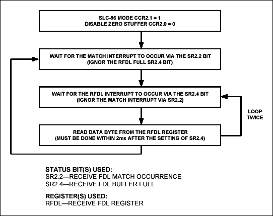
Figure 1. SLC-96 Message field extraction via RFDL.
Figure 2 details how the SLC-96 fields will be represented in the RFDL register on each read. Since the RFDL is also used in the ESF framing mode, the zero destuffer should be disabled (CCR2.0 = 0). (Note: The match registers (RFDLM1 and RFDLM2) are not used in SLC-96 mode and can be programmed with any value.)

Figure 2. RFDL Register byte sequence.
Figure 3 displays the method to enable the device to insert the SLC-96 message fields via the TFDL register. On each normal D4 multiframe boundary, the framer will signal to the user via the SR2.6 bit to write to the TFDL the sequence of bytes shown in Figure 4. The user will write to the TFDL six times in each SLC-96 multiframe.
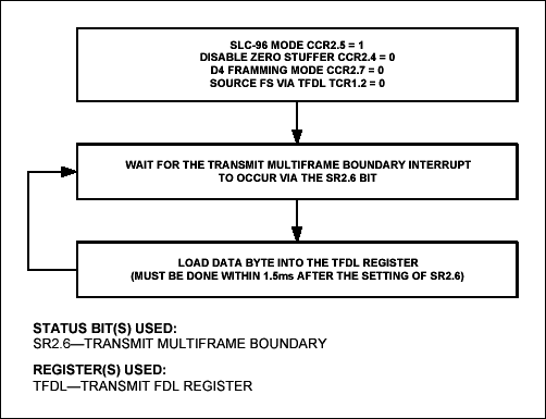
Figure 3. SLC-96 Message field insertion via TFDL.
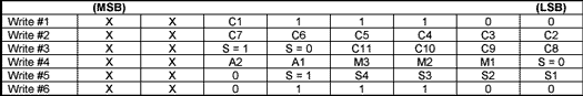
Figure 4. TFDL Register byte sequence.
If you have further questions concerning the operation of Dallas Semiconductor's T1/E1 framers and single-chip transceivers, please contact the Telecommunication Applications support team via email telecom.support@dalsemi.com or call 972-371-6555.
打开APP阅读更多精彩内容
Introduction
This application note applies to the following products:| T1 Framers | T1 SCTs |
| DS2141A | DS2151 |
| DS21Q41B | DS2152 |
| DS21Q42 | DS21352 |
| DS21FF42 | DS21552 |
| DS21FT42 | DS21Q352 |
| DS21Q552 |
In a SLC-96-based transmission scheme, the standard Fs-bit pattern is robbed to make room for a set of message fields. The SLC-96 multiframe is made up of six D4 superframes, so it is 72 frames long. In the 72-frame SLC-96 multiframe, 36 of the framing bits are the normal Ft pattern and the other 36 bits are divided into alarm, maintenance, spoiler, and concentrator bits, as well as 12 bits of the normal Fs pattern. Please see the Bellcore document TR-TSY-000008 for more details about SLC-96.
Receive-Side SLC-96 Applications
To enable the device to synchronize onto a SLC-96 pattern, the following configuration should be used:- Set to D4 framing mode (CCR2.3 = 0)
- Set to cross-couple Ft and Fs bits (RCR1.3 = 1)
- Set to minimum sync time (RCR1.2 = 0)
Figure 1 describes the method used to extract the SLC-96 message bits. The devices contain an on-board SLC-96 synchronizer that is enabled when the CCR2.1 bit is set to one. In this mode, the match flag (SR2.2) takes on a new meaning; it will indicate when the framer has received the 12-bit Fs pattern that exists in SLC-96 multiframe. In each SLC-96 multiframe, the user will read the RFDL register three times. The external controller will wait for the match flag to be set. Once set, the controller will then wait for the RFDL to fill.
Figure 1. SLC-96 Message field extraction via RFDL.
Figure 2 details how the SLC-96 fields will be represented in the RFDL register on each read. Since the RFDL is also used in the ESF framing mode, the zero destuffer should be disabled (CCR2.0 = 0). (Note: The match registers (RFDLM1 and RFDLM2) are not used in SLC-96 mode and can be programmed with any value.)
Figure 2. RFDL Register byte sequence.
Transmit-Side SLC-96 Applications
To insert the SLC-96 message fields, the user has the option to either use the external TLINK pin or to use the onboard TFDL register. Usage of the TLINK pin will require some external hardware and to enable this option, the TCR1.2 bit should be set to one. This application note concerns itself solely to the use of the TFDL register to insert the SLC-96 message fields.Figure 3 displays the method to enable the device to insert the SLC-96 message fields via the TFDL register. On each normal D4 multiframe boundary, the framer will signal to the user via the SR2.6 bit to write to the TFDL the sequence of bytes shown in Figure 4. The user will write to the TFDL six times in each SLC-96 multiframe.
Figure 3. SLC-96 Message field insertion via TFDL.
Figure 4. TFDL Register byte sequence.
T1 Framer And Single-Chip Transceiver Information
For more information about Dallas Semiconductor's T1/E1 framers and single-chip transceivers, please consult the data sheets available on our website at www.maxim-ic.com/telecom.If you have further questions concerning the operation of Dallas Semiconductor's T1/E1 framers and single-chip transceivers, please contact the Telecommunication Applications support team via email telecom.support@dalsemi.com or call 972-371-6555.
声明:本文内容及配图由入驻作者撰写或者入驻合作网站授权转载。文章观点仅代表作者本人,不代表电子发烧友网立场。文章及其配图仅供工程师学习之用,如有内容侵权或者其他违规问题,请联系本站处理。
举报投诉
- 相关推荐
- 热点推荐
- Programmin
-
DS2152L与DS2151Q的比较2023-06-13 2096
-
DS21352/DS21552与DS2152单芯片收发器的比较2023-02-07 2231
-
为下一代器件提供DS2152或DS2154硬件设计2023-01-13 1885
-
DS21352/DS21552与DS2152单芯片收发器-D2009-04-29 768
-
DS2152, DS2154, DS2151, DS21532009-04-20 1099
全部0条评论

快来发表一下你的评论吧 !
