

倍频器使用延迟线
通信设计应用
65人已加入
描述
Abstract: Any independent delay line, in conjunction with a XOR gate, can be made into a clock frequency doubler by delaying the clock signal, and combining the delayed clock signal with the undelayed signal using the external logic. This application brief demonstrates how it can be done with a DS1035. The technique works with the DS1100 and DS1135 series as well.
If a clock signal is delayed by one-quarter period, it can be gated with the original waveform to produce a novel application: frequency-doubled output.
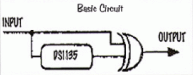
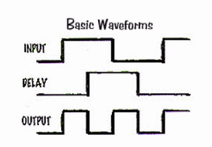
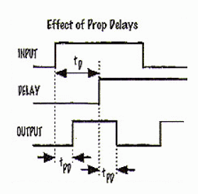
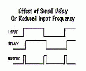
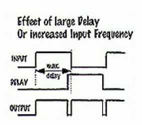
This time, the XOR propagation delay (tPD) will impact only the relative skew from input to output and will not otherwise distort the waveform. Obviously, the optimum delay time for this application is one-quarter of the input period. Deviation from this "ideal" value, or altering the input frequency, will cause a change in the output duty cycle but will not change the frequency. The minimum usable delay (lowest usable input frequency) is dependent only on the minimum acceptable output pulse width or duty cycle. The maximum usable delay (highest input frequency) is constrained by the minimum input pulse width specification of the delay line.
打开APP阅读更多精彩内容
If a clock signal is delayed by one-quarter period, it can be gated with the original waveform to produce a novel application: frequency-doubled output.


This time, the XOR propagation delay (tPD) will impact only the relative skew from input to output and will not otherwise distort the waveform. Obviously, the optimum delay time for this application is one-quarter of the input period. Deviation from this "ideal" value, or altering the input frequency, will cause a change in the output duty cycle but will not change the frequency. The minimum usable delay (lowest usable input frequency) is dependent only on the minimum acceptable output pulse width or duty cycle. The maximum usable delay (highest input frequency) is constrained by the minimum input pulse width specification of the delay line.


声明:本文内容及配图由入驻作者撰写或者入驻合作网站授权转载。文章观点仅代表作者本人,不代表电子发烧友网立场。文章及其配图仅供工程师学习之用,如有内容侵权或者其他违规问题,请联系本站处理。
举报投诉
-
Custom MMIC倍频器的主要特征2021-09-11 805
-
Data Delay Device, Inc模拟和数字延迟线以及延迟线应用模块和滤波器的设计者2021-06-04 1087
-
电视机的亮度延迟线的制作方法分享2021-05-24 1871
-
关于延迟线的问题2020-06-07 2225
-
倍频器分类2019-01-08 7240
-
亮度与色度延迟线的选用、检测与代换2012-06-19 2773
-
亮度延迟线电路2012-02-22 3167
-
有谁使用过延迟线······2011-09-05 3575
-
延迟线电路,延迟线电路是什么意思2010-03-09 1679
-
Dallas Semiconductor的延迟线如何工作?2009-04-29 757
-
数字倍频器2009-04-11 1644
-
Dallas Semiconductor的延迟线如何工作2009-03-23 897
全部0条评论

快来发表一下你的评论吧 !

