

驱动LED与推挽输出端口扩展器-Driving LEDs w
通信设计应用
描述
The Basics
The standard connection for driving an LED from a port is shown in Figure 1. The load is typically a single LED, but can be dual LEDs in series, as shown, depending on the choice of LEDs and supply voltage. The series resistor R1 is necessary to limit the current through the LED. The value of resistor R1 required to drive a current IPORT through the LED can be calculated using the formula:R1 or R2 = (V+ - VPORT - VLED) / IPORT ohms
where V+ is the I/O expander and LED supply voltage
VLED is the voltage drop across the LED(s) at the required load current (usually in the range 1.8V to 2.4V for red LEDs, and 3V to 4.2V for blue, white, and high efficiency green LEDs)
VPORT is the voltage drop across the output port when sinking the required load current (for example 0.25V at 20mA for MAX7310)
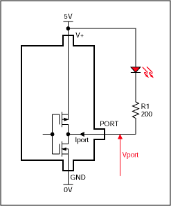
Figure 1. Standard LED connection.
The LED current will vary with supply voltage and LED forward voltage. Resistor initial accuracy and temperature coefficient, plus any variance in port output voltage with temperature and supply voltage, will also play a part. If consistent LED current is important, make sure that the voltage drop across resistor R1 is high compared with the total voltage variances in supply and LED. For example, consider a situation where we need to drive a nominal 20mA through a red LED whose forward voltage is 2V ±0.2V. We have a choice of 3.3V ±5% or 5V ±5% supplies, and a 5V I²C bus. A MAX7310 will work on either supply with a 5V I²C bus, because its I²C interface is overvoltage protected. The MAX7310 port will drop 0.2V ±0.1V when sinking 20mA.
Using the typical values, the value for R1 calculates to be (5 - 2 - 0.2) / 0.02 = 140 for the 5V supply case, and (3.3 - 2 - 0.2) /0.02 = 55
 for the 3.3V case. Using these exact values for R1, then the actual current variation at the tolerance extremes would be ±3.9mA (a 19.5% variation) for the 5V case, and ±8.5mA (a ±42% variation) for the 3.3V case. Clearly the 3.3V solution has a much wider current variation than the 5V solution. However, the 5V solution dissipates more power in the current limiting resistor. If this current variation is too high, consider using a port expander with constant-current (internally current limited) outputs such as MAX6956 and MAX6957, or use techniques such as shown in Figures 7 to 12 which use an external transistor to control the current more accurately.
An alternative standard LED connection is shown in Figure 2, and in this case the port is sourcing current instead of sinking it. As a rule, the Figure 1 'sink' drive is preferred to the Figure 2 'source' drive because most ports (and logic outputs for that matter) can sink more current than they can source. Also, the driver voltage drop is usually higher across the current sourcing PFET than the current sinking NFET for the same current. The Figure 2 circuit does have the advantage that the LED cold end is grounded, usually simplifying PCB layout slightly. Also, the true logic operation (a high output lights the LED) may ease the software implementation.
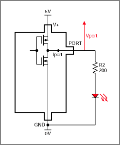
Figure 2. Alternative LED connection.
Note that cold ends of the LEDs in the circuits of Figure 1 and Figure 2 are connected to one of the port expander supply pins, V+ or GND. The protection diodes within the push-pull output structure of a CMOS driver disallows connection of a load referred to a voltage outside the supply range. However, it is possible to connect the LED in the Figure 1 circuit to a lower voltage such as 3.3V instead of the 5V port expander supply. This would save some power dissipated in resistor R1, but increase the LED current variation due to supply and other tolerances as discussed earlier.
Driving LEDs in Parallel
Multiple LEDs can be driven in parallel to share the current from a single output (Figure 3). The 'ballast' resistors R3 and R4 assist the current balancing between the LEDs if their forward voltages aren't well matched. In many cases, modern LEDs of the same type and manufacturer are matched well enough that the resistors can be omitted with negligible intensity mismatch. Driving LEDs in parallel as opposed to in series reduces the drive voltage required, reduces the drive current available for each LED.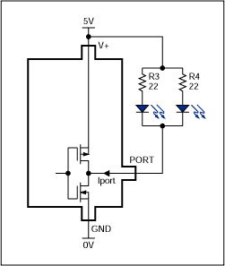
Figure 3. Driving multiple LEDs from one output.
Want More LED Current? Use More Ports
If more load current is required than is available from one port, multiple ports can be paralleled in a wire-OR fashion to drive a single load. Because the outputs are push-pull and not current limited, the paralleled outputs need to be turned on simultaneously to the same level, or prevented from shorting if they happen to be at opposite levels at any time. A safe way of avoiding shorts is to use a separate current limiting resistor per port (Figure 4). If the two ports are switched to opposite levels, resistors R5 and R6 limit the current passing from the high output to the low output. Power is wasted, but the ports are protected. When both outputs are low, the resistors set the LED current to a safe level for each output.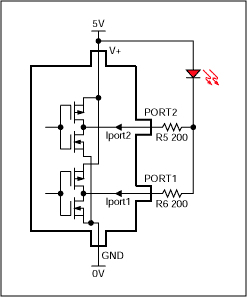
Figure 4. Paralleling outputs - the safe way.
An alternative approach is to guarantee that the paralleled ports are switched together. Many port expanders (MAX7300, MAX7301, MAX7310 and MAX7311 included) use a register structure that allows multiple outputs to be switched simultaneously with the same software command. If this is the case, it becomes a software issue to ensure that the ports will always be set to the same level, and the circuit of Figure 5 can be used. Remember that programming the ports to opposite logic levels will directly short the outputs...
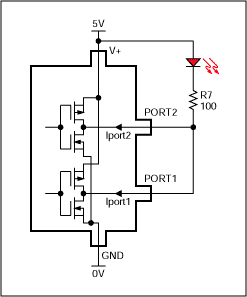
Figure 5. Paralleling outputs - the lower cost way.
Even More LED Drive Voltage or Current? Add a Transistor
As discussed earlier, output loads must not be connected to a voltage outside the port expander's supply range. This becomes a problem if the port expander is being operated from a low voltage insufficient to drive LEDs, such as 2.5V. Even the usual 5V maximum supply voltage may not be enough to drive a single blue or white LED, or two red LEDs in series. The circuits shown in Figures 6 to 12 use an external transistor to to extend the voltage drive and/or the drive current.The first two circuits uses a single transistor switch which essentially replaces the port expander's output driver (Figures 6 and 7). The transistor ratings alone determine how much LED current and voltage can be handled. Advantages of this circuit compared with the circuits discussed next are low wasted voltage across the transistor switch because it is turned on hard, and the LED current will not vary with port expander supply voltage. Disadvantages are that LED current will vary with the VEXT supply voltage, and that the circuit uses two resistors.
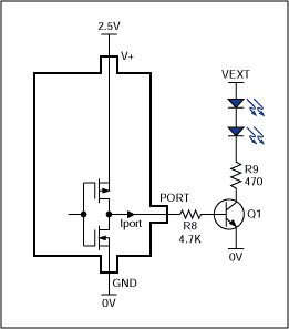
Figure 6. Driving LEDs with higher current and a positive voltage.
The circuit of Figure 6 allows any positive voltage to be used for VEXT. The circuit of Figure 7 allows any negative voltage to be used, and has the advantage that the LED current flows from the port expander supply to the negative supply, making the sum of the two supplies available to drive the LEDs.
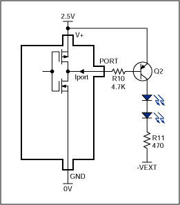
Figure 7. Driving LEDs with higher current and a negative voltage.
What about Constant Current?
The LED drive current in the circuits of Figure 6 and 7 varies with LED supply voltage, VEXT. If VEXT is not well regulated, this could be a problem. In the circuit of Figure 8, Q3 operates as a common-base (cascode) current switch. The port output VPORT is constrained to a safe voltage of (V+ - VBE) because Q3's base is tied to the driver supply voltage, V+. Q3's emitter current IPORT can be calculated using the formula:IPORT = (V+ - VPORT - VBE) / R12 Amps
The port current Iport (also Q3's emitter current) will flow through Q3's collector and the LED loads, less a small base current taken by Q3. The current error due to Q3's base current can be kept below 1% by choosing a reasonably high gain (ß > 100) transistor for Q3. If supply voltage V+ doesn't vary much (VPORT and VBE won't), then this circuit works as a pretty good constant current sink, dependent on the port expander supply voltage, but independent of the LED supply voltage VLED.
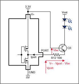
Figure 8. Active-low, constant current sink LED drive.
One disadvantage of the Figure 8 circuit is that the LED load current flows through the port expander active low output, thereby limiting the maximum LED current to that of the port expander. The Figure 9 circuit avoids this problem, and allows the current as well as the voltage rating to be determined by the transistor ratings. Q4's emitter current ILED can be calculated using the formula:
ILED = (V+ - VBE) / R13 Amps
In the Figure 9 circuit the port expander active high output is supplying Q4's base current only, which is small enough that the port output voltage drop is negligible and is ignored.
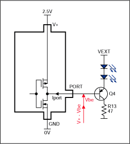
Figure 9. Active-high, constant current sink LED drive.
Figures 10 and 11 show mirror topologies of the Figures 8 and 9 circuits with PNP pass transistors replacing the NPNs. Now the LEDs are referred to a negative supply instead of a higher voltage positive supply. LED current is supplied from the port expander's positive supply and returned into the negative supply.
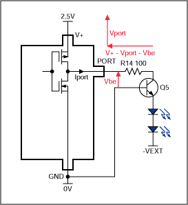
Figure 10. Active-high, constant current source LED drive.
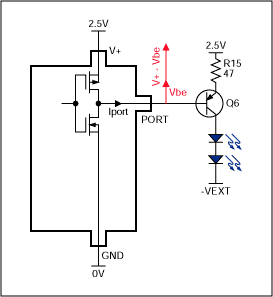
Figure 11. Active-low, constant current source LED drive.
A limitation of the Figure 8 circuit is that the collector of the external transistor Q3 can go no lower than (V+ - VBE + VCE(sat)), which is only a little below V+. If V+ is high, for example 5V, then not only is the output expander dissipating a high power due to this high voltage drop forced across its output, but also the voltage headroom available for the LEDs is reduced to almost (VEXT - V+). A simple solution is to bias the pass transistor's base to a lower voltage using a series zener diode. Only one zener diode is needed to serve multiple pass transistors, as shown in the Figure 12 circuit. With this circuit Q7's and Q8's emitter voltage sit at about 1.6V when the supply voltage V+ is 5V. The mirror circuit of Figure 10 can be modified in the same way also, but the Figure 9 and Figure 11 circuits will need a separate zener in series with the base of each transistor.
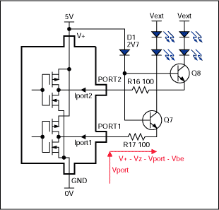
Figure 12. Using a zener diode to minimize driver headroom.
-
使用端口扩展器轻松高效地向IIoT端点添加具有成本效益的子节点2020-06-16 0
-
ATtiny GPIO扩展器的资料下载2022-07-12 0
-
利用微型端口扩展器控制LED2006-03-24 575
-
端口扩展器降低折叠手机的成本及尺寸2009-04-29 1227
-
扩展器输出驱动器电路图2009-06-10 2676
-
ADI推出通用输入/输出端口扩展器和键盘矩阵控制器ADP5585和ADP55892011-09-14 1650
-
MAX6957 LED显示驱动器及输入/输出扩展器典型应用电路2012-05-17 1875
-
ADP5586原文资料数据手册PDF免费下载(键盘解码器和I/O端口扩展器)2017-10-27 778
-
基于 MCU 设计的I²C 和 SPI 扩展器2022-08-15 1492
-
使用Galileo II和ANSI C驱动MCP23017 IO扩展器16个通用输出2022-10-21 526
-
驱动具有恒流端口扩展器输出的LED2023-03-01 1000
-
用于翻盖手机的端口扩展器可节省成本和空间2023-03-08 923
-
串行端口扩展器-带有PIC MCU的额外SPI和UART端口2023-07-12 365
-
信路达 I/O端口扩展器 XL8574AT数据手册2022-08-19 323
全部0条评论

快来发表一下你的评论吧 !

