

Timing Considerations When Usi
嵌入式新闻
7人已加入
描述
Abstract: This article assists in preparing the system memory timing for use with Dallas Semiconductor's Nonvolatile SRAM (NVSRAM). Refer to the product data sheets for the referenced timing diagrams and minimum allowable delay values for each relevant parameter.
Dallas Semiconductor's NVSRAM modules are constructed using a Dallas nonvolatile controller, a low-power CMOS Static RAM memory component, and a lithium coin-cell battery. Under normal operating conditions, read or write operations are functionally identical to a stand-alone SRAM. Using the parallel I/O structure, a user can easily store data to, or fetch data from any memory location defined by the address bus width. Subsequent memory cycles can occur at this, or any other location in any order desired with no duty cycle or write cycle-count restrictions.
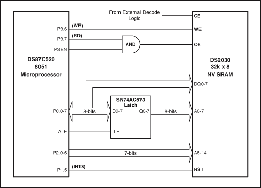
Figure 1. Typical NVSRAM circuit.
If the system power is above the specified Write-Protect Voltage (VTP), the three control input pins (active-low CE, active-low WE, and active-low OE) define the memory operation to be performed, as depicted in Table 1. Write commands have priority over read commands. Maximum current consumption (ICC) for each state is specified in the DC Electrical Characteristics table in the product's data sheet.
Table 1. Operational Truth Table
x = Do not care
ICCS1 or ICCS2 is dependent upon the Input Voltage Levels (VIH/VIL) used.
When defining system memory timing, it is also important to remember that an SRAM acts similar to a 'latch with depth'. You have to present your inputs (address and data) before you enable the controlling clock signal. This is defined as "setup time." You must also maintain that input condition (address and data) until the 'latch' operation completes. This is defined as "hold time." Hold times can vary according to which clock input is selected as the controlling signal.
For a successful write operation to occur, the following conditions must be met:
With NVSRAM, there is an internal propagation delay exclusively through the active-low CE path. If using active-low WE to define the start and/or end points, follow the minimum timing requirements in the data sheet for the Write Cycle 1 illustration. If using active-low CE to define the start and/or end points, follow the minimum timing requirements in the data sheet for the Write Cycle 2 illustration.
Also remember that digital signals do not jump instantaneously from a logic 0 to a logic 1, as sometimes depicted in timing diagrams. Input-signal transition times can be difficult to predict at the system design stage, as that load characteristic is heavily dependant upon PC-board component placement, routing, and materials. To enhance the operational noise immunity in the final application, it is suggested that system setup and hold time delays exceed the data sheet minimums.
For a successful read operation to occur, these conditions must be met:
During a valid read, any address change that occurs prior to the expected read access time (active-low CE to Output Valid) prematurely terminates this memory cycle. When the address lines are again stable, the new address presented will trigger a 'new' read cycle. The data from the first address are not guaranteed to be presented at the I/O pins. The data from the 'new' address will be presented at the I/O pins by the address-activated access time (Access Time), from the point at which the last address input became stable.
The I/O pins will drive data only when ((valid read) AND (active-low OE = 0)). This may be important for power consumption, as reduced device duty cycles and delayed output gating can reduce the component's current consumption.
If you have questions/comments/suggestions about this application note, please send them t MixedSignal.Apps@dalsemi.com.
Notes:
打开APP阅读更多精彩内容
Dallas Semiconductor's NVSRAM modules are constructed using a Dallas nonvolatile controller, a low-power CMOS Static RAM memory component, and a lithium coin-cell battery. Under normal operating conditions, read or write operations are functionally identical to a stand-alone SRAM. Using the parallel I/O structure, a user can easily store data to, or fetch data from any memory location defined by the address bus width. Subsequent memory cycles can occur at this, or any other location in any order desired with no duty cycle or write cycle-count restrictions.
Figure 1. Typical NVSRAM circuit.
If the system power is above the specified Write-Protect Voltage (VTP), the three control input pins (active-low CE, active-low WE, and active-low OE) define the memory operation to be performed, as depicted in Table 1. Write commands have priority over read commands. Maximum current consumption (ICC) for each state is specified in the DC Electrical Characteristics table in the product's data sheet.
Table 1. Operational Truth Table
| VCC | Active-Low CE | Active-Low WE | Active-Low OE | Address Bus | DQ Bus | Function | ICC |
| < VTP | x | x | x | x | High impedance | Write-protect | n/a |
| > VTP | 1 | x | x | x | High impedance | Standby | ICCS1 or ICCS2 |
| 0 | 1 | 1 | Stable | High impedance | Read | ICCO1 | |
| 0 | 1 | 0 | Stable | Output data | Read | ICCO1 | |
| 0 | 0 | x | Stable | Input data | Write | ICCO1 |
x = Do not care
ICCS1 or ICCS2 is dependent upon the Input Voltage Levels (VIH/VIL) used.
Suggested Rules for Robust Functional Operation
Three primary rules must always apply to any valid memory operation:- VCC must be greater than the specified Write-Protect Voltage (VTP) throughout the active memory cycle.
- The address bus must be stable throughout the active memory cycle.
- Cycle time of the active memory cycle (tRC or tWC) should meet or exceed the minimum specified times listed in the data sheet.
Understand the Timing Diagrams
It is important to remember that data-sheet timing diagrams generally show only one data line or address line in the depiction. In reality, you are providing at least eight data lines and over a dozen address lines probably with different signal-path lengths on the system board, and potentially with different loading characteristics on each signal. With a purely static memory, the last address and/or data signal to arrive at the device's input pins are the only ones that really count. The first address and/or data signal to change at the end of this memory operation are, again, the only ones that really count. Consequently, to avoid a classic timing race, take a few simple precautions in the timing definitions.When defining system memory timing, it is also important to remember that an SRAM acts similar to a 'latch with depth'. You have to present your inputs (address and data) before you enable the controlling clock signal. This is defined as "setup time." You must also maintain that input condition (address and data) until the 'latch' operation completes. This is defined as "hold time." Hold times can vary according to which clock input is selected as the controlling signal.
Write Cycles
As illustrated in Table 1, a valid write exists when ((active-low CE = 0) AND (active-low WE = 0)).For a successful write operation to occur, the following conditions must be met:
- The device must be enabled at the selected address for a minimum time (Write Cycle).
- The write function must be enabled for a minimum time (Write Pulse Width).
- The I/O pins (DQ0 through DQ7(1)) must be driven to a valid condition prior to (Data Setup), and held stable for some time after (Data Hold) the end point.
A write cycle starts when valid write becomes TRUE. It is performed at the address presented on the address pins. The start point is defined as the later occurring falling edge of either active-low CE(2) or active-low WE(3).
A write cycle ends when valid write becomes FALSE. The end point is defined as the earlier occurring rising edge of either active-low CE(2) or active-low WE(3).
With NVSRAM, there is an internal propagation delay exclusively through the active-low CE path. If using active-low WE to define the start and/or end points, follow the minimum timing requirements in the data sheet for the Write Cycle 1 illustration. If using active-low CE to define the start and/or end points, follow the minimum timing requirements in the data sheet for the Write Cycle 2 illustration.
Also remember that digital signals do not jump instantaneously from a logic 0 to a logic 1, as sometimes depicted in timing diagrams. Input-signal transition times can be difficult to predict at the system design stage, as that load characteristic is heavily dependant upon PC-board component placement, routing, and materials. To enhance the operational noise immunity in the final application, it is suggested that system setup and hold time delays exceed the data sheet minimums.
Read Cycles
As illustrated in Table 1, a valid read exists when ((active-low CE = 0) AND (active-low WE = 1)), but no data out will appear unless active-low OE = 0.For a successful read operation to occur, these conditions must be met:
- The device must be enabled at the selected address for a minimum time (Read Cycle).
- The write function must be disabled.
- The I/O pins (DQ0 through DQ7(1)) must be gated on for a minimum time (active-low OE to Output Valid) at or after the expected read access time (active-low CE to Output Valid).
A read cycle starts when valid read becomes TRUE. It is performed at the address presented on the address pins. The I/O pins become low impedance if active-low OE is also low(4).
A read cycle ends when valid read becomes FALSE. The I/O pins become high impedance if active-low OE is also low(4).
During a valid read, any address change that occurs prior to the expected read access time (active-low CE to Output Valid) prematurely terminates this memory cycle. When the address lines are again stable, the new address presented will trigger a 'new' read cycle. The data from the first address are not guaranteed to be presented at the I/O pins. The data from the 'new' address will be presented at the I/O pins by the address-activated access time (Access Time), from the point at which the last address input became stable.
The I/O pins will drive data only when ((valid read) AND (active-low OE = 0)). This may be important for power consumption, as reduced device duty cycles and delayed output gating can reduce the component's current consumption.
If you have questions/comments/suggestions about this application note, please send them t MixedSignal.Apps@dalsemi.com.
Notes:
- For the DS1258, this applies to DQ0 through DQ15. For the DS2227 this applies to DQ0 through DQ31. For the DS38464, this applies to DQ0 through DQ39.
- For the DS1258, this applies to active-low CEL or active-low CEU. For the DS2227, this applies to 1- active-low CE through 4- active-low CE. For the DS38464, this applies to active-low CEA.
- For the DS2227, this applies to 1- active-low WE through 4- active-low WE.
- For the DS2227, this applies to 1- active-low OE through 4- active-low OE.
声明:本文内容及配图由入驻作者撰写或者入驻合作网站授权转载。文章观点仅代表作者本人,不代表电子发烧友网立场。文章及其配图仅供工程师学习之用,如有内容侵权或者其他违规问题,请联系本站处理。
举报投诉
- 相关推荐
- 热点推荐
- nvSRAM
-
oracle case when 语法介绍2023-12-06 4014
-
时序分析基本概念介绍—Timing Arc2023-07-06 6131
-
什么是时序路径timing path呢?2023-07-05 3560
-
Timing Commander 软件 for Programmable Buffers2023-05-15 437
-
怎么设置和重置XIL_TIMING_ALLOW_IMPOSSIBLE2019-03-05 3400
-
Perfect Timing II Book2017-10-27 910
-
attiny usi 做IIC通信,怎么用。新手!2013-12-03 2323
-
Jitter Analysis Techniques Usi2010-07-19 478
-
Important considerations for i2010-05-14 1207
-
Security Considerations for Vo2010-04-27 557
-
Achieving Timing Closure2010-01-11 1062
-
Thermal Considerations2009-11-29 928
-
Design Considerations for Dall2009-03-31 1279
-
Power considerations when usin2009-03-29 691
全部0条评论

快来发表一下你的评论吧 !
