
The Advantages of Using Low-Vo
通信设计应用
65人已加入
描述
The choice of SCSI (Small Computer System Interface) transceivers, whether single-ended (SE) or differential (HVD or LVD), determines the speed of data transfers, the length of cable, and the number of devices that can be supported by a host controller.
Since its inception in 1981, SCSI1, now referred to as SCSI-1, relied exclusively upon single-ended 8-bit wide bus transceivers for host-to-peripheral data transfers. While SCSI-1 is defined with speeds up to 5 megabytes per second, SCSI-2 offers speeds up to 10 megabytes per second with optional high voltage differential drivers (HVD) and a wide (16-bit wide) data bus. SCSI-3 SPI extends the evolution to 20 megabytes per second with a wide HVD bus. With the advent of Ultra SCSI, Ultra2, Ultra 160, and now Ultra 320, data bus transfers can reach up to 320 megabytes per second. (See Table 1 below).
Table 1. STA-Endorsed Terms & Terminology for SCSI
打开APP阅读更多精彩内容
Since its inception in 1981, SCSI1, now referred to as SCSI-1, relied exclusively upon single-ended 8-bit wide bus transceivers for host-to-peripheral data transfers. While SCSI-1 is defined with speeds up to 5 megabytes per second, SCSI-2 offers speeds up to 10 megabytes per second with optional high voltage differential drivers (HVD) and a wide (16-bit wide) data bus. SCSI-3 SPI extends the evolution to 20 megabytes per second with a wide HVD bus. With the advent of Ultra SCSI, Ultra2, Ultra 160, and now Ultra 320, data bus transfers can reach up to 320 megabytes per second. (See Table 1 below).
Table 1. STA-Endorsed Terms & Terminology for SCSI
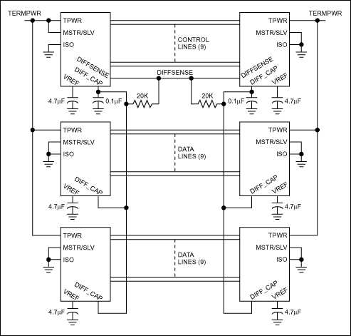
The LVD SCSI, introduced in 1995, provides the low power, low cost of single-ended transceivers with the signal integrity, along with high-speed capability of HVD SCSI. Each LVD (V+ and V-) signal swings about +400mV around a common mode bias voltage of 1.25V. This small amount of change allows the signal to achieve its desired state more quickly than in single-ended or high voltage differential signaling. With LVD SCSI, based upon the EIA-644 (LVDS) standard for data transmissions over a copper wire, speeds of up to 655 megabytes per second can be reached (point-to-point). Another advantage of LVD SCSI over HVD SCSI is it's backward compatibility to SE SCSI2. Speed and distance for SE and HVD are not defined for Ultra3 or Ultra 160 and beyond. Specifications beyond Ultra 160 are clearly defined only for LVD, see Table 1 The DS2120 LVD SCSI terminator is fully compliant with Ultra320, Ultra3 or Ultra160, and Ultra 2 (LVD only) SCSI interface requirements. Since the DS2120 is an LVD-only SCSI terminator, SE or HVD devices connected to the bus with cause the DS2120 to automatically disconnect from the bus. This is accomplished inside the part automatically by sensing the voltage on the DIFFSENS line. LVD termination is provided by 5% tolerance laser-trimmed resistors biased with two current sources and a common-mode voltage source generated from a bandgap reference of 1.25V. The configuration is a y-type terminator with a 105Ω differential and a 150Ω common-mode resistance. A failsafe bias of 112mV is maintained when no drivers are connected to the LVD SCSI bus. Another failsafe is the bandgap temperature-to-voltage converter used to determine when the device exceeds 150°C. Once thermal shut-down temperature is reached, the device is electrically isolated from the bus. The DIFF_CAP pin monitors the DIFFSENS line to determine the proper operation mode of the device. If the voltage on the DIFF_CAP is between 0.7V and 1.9V, the device enters LVD mode after the mode-change delay. Three DS2120 LVD terminators are needed for wide SCSI applications (See Figure 1). In a typical application the SCSI devices are daisy-chained as shown below. The DIFFSENSE pin can also drive the SCSI DIFFSENS line when (MSTR/SLV) = 1) to determine the proper operating mode.  Figure 1. SCSI wide bus configuration. Internal to these devices, there is a 75KΩ pull-up between TPWR and the MSTR/SLV lines. Because of the internal pull-up, the MSTR/SLV line can be tied high, as shown in Figure 1 or optionally it can be left floating3. The DS2120 is a high-performance LVD SCSI terminator. It is designed to provide the speed of HVD SCSI terminators, without the associated power consumption and real estate requirements. In the above configuration, only one set of terminators would typically reside on the host bus adapter (HBA), while the other set would exist in a small connector package at the end of the SCSI cable. The DS2120E resides in a small 28-pin 4.4mm TSSOP package. The complete packaging solution can easily be designed onto the end of a cable assembly or a cable adapter. The DS2120 also provides low power-down capacitance of 3pF and is hot-plug compatible. The operating ranges are from 2.7V to 5.5V and 0°C to 70°C. Footnotes
| ||||||||||||||||||||||||||||||||||||||||||||||||||||||||||||||||||||||||||||||||||||||||||||||
声明:本文内容及配图由入驻作者撰写或者入驻合作网站授权转载。文章观点仅代表作者本人,不代表电子发烧友网立场。文章及其配图仅供工程师学习之用,如有内容侵权或者其他违规问题,请联系本站处理。
举报投诉
- 相关推荐
- 热点推荐
- L
-
CN0545: Completely Integrated, 0.1°C Thermistor Measurement System Using a Low Power, Precision, 24-Bit Sigma-Delta ADC2021-01-28 705
-
SMBus Design Using Low Power Microcontroller2015-03-23 4828
-
ADG774A,pdf datasheet ( Low Vo2009-10-30 761
-
ISL54208,pdf,datasheet (Low Vo2009-09-11 559
-
A Low-Noise-Amplifier with good IP3outperformance at 1.9 GHz using BFP4202009-05-12 2786
-
Advantages Of An Automated Set2009-05-08 630
-
Temperature Monitoring Using t2009-04-17 2433
-
12-Bit Thermometer Using an 8-2009-03-31 952
-
MAX17083 pdf datasheet (Low-Vo2009-03-02 569
-
ISL43210 pdf datasheet (Low-Vo2009-02-07 622
-
Advantages of Using a MicroMonitor and a Simple Application Demonstrating the2008-09-24 5581
全部0条评论

快来发表一下你的评论吧 !

