
One Button Turns Microprocesso
电源新闻
描述
When placing a microprocessor-based portable device in your desk drawer for weeks or months, you should, of course, turn it off to save battery capacity (unless it requires power to maintain storage of volatile data or to keep a real-time-clock running). To save as much power as possible, it's usually best to turn off the processor, its peripherals, and all power-supply components.
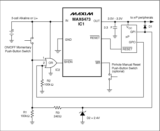
A simple circuit (Figure 1) enables a single pushbutton to turn the power off and on. It includes a single OR gate (IC1) and a second device (IC2) that combines a low-dropout linear regulator with microprocessor-reset circuit in a SOT23, QFN, or ultra-chip-scale package.

Figure 1. This 1-button turn-on/turn-off circuit is implemented with an LDO and a single OR gate.
The single-gate OR circuit (TinyLogic™ NC7SZ32 in SC70 or chip-scale package) features low quiescent current, and is the only circuit powered during the OFF time. A user turns the device on by closing the ON/OFF pushbutton switch, which produces a logic high at input 1 of the OR gate. The gate output drives the LDO's SHDN input high, causing the LDO output to ramp up toward its preset voltage.
The LDO RESET output of IC2 remains low until the LDO output voltage has stabilized for the desired reset timeout period. When IC2 de-asserts its RESET output, the processor initiates code execution and drives a general-purpose output (GPO) high. With GPO high, the device remains in power-ON mode when the pushbutton is released, but to ensure a proper turn-on sequence the ON/OFF pushbutton must remain closed for an interval that includes the LDO turn-on time (100s of microseconds), the reset timeout period (100s of milliseconds to 10s), and the code-execution time for GPO high (100s of microseconds to one millisecond). To minimize the possibility of accidental turn-on due to a short pushbutton closure, include a delay of several seconds between the processor's emergence from reset and the GPO output's transition to high. (The LDO and µP power up when the switch is closed, but will automatically turn off unless the pushbutton remains closed for several seconds.)
The µP's general-purpose input (GPI) is low during normal operation, and is monitored by the µP for a low-to-high transition. To initiate a power-OFF sequence, drive GPI high by closing the ON/OFF switch. Use processor code to de-bounce the switch and to monitor the GPI input for the desired turn-off timeout period. (That is, wait for the switch to remain closed for a few seconds before shutting down the device.)
When the processor has validated the pushbutton power-down condition it drives GPO low, and when the pushbutton is released the OR gate output goes low, shutting down the LDO and putting the device in a low-power shutdown mode. To ensure turn off when a user forgets to turn the device off manually, you can program the processor to turn off the LDO by driving GPO low, following a period of several minutes with no user activity. Because GPI is high for both turn-on and turn-off, you need state-based processor code to interpret the appropriate GPO response. R1 and R2 ensure that the OR-gate inputs remain low during the power OFF mode.
Becsuse the pushbutton switch monitors switch closure by connecting battery voltage to the GPI input, additional voltage-protection circuitry may be required for some µPs. During normal operation, zener diode D2 and resistor R3 limit the GPI input to a level below the µP's Vcc voltage. Select a zener voltage below the nominal Vcc level and above the logic high level for the µP's GPI input. During initial power-up, the GPI input approaches Vzener before the LDO output turns on (the µP Vcc equals 0V). Combined with resistor R3, a low-voltage zener diode (D2) from GPI to Vcc limits voltage and current at the GPI input until Vcc is fully powered. That diode also helps to pull Vcc up when the pushbutton switch is closed. (If the processor inputs tolerate high voltage, you can remove D1 and D2.)
This circuit may fail to respond to ON/OFF pushbutton commands if the processor does not include an internal watchdog timer, and therefore fails to execute code properly during ON mode. You can preclude this problem by adding an optional pinhole reset, which allows the user to re-establish device control by resetting the µP. The pinhole reset ties directly to IC2's manual reset input, and requires no external debounce circuitry. When closed, the pinhole pushbutton forces the µP into reset, allows GPO to go low, and turns off the LDO. You can then re-power the device via the ON/OFF button.
The Figure 1 circuit accepts a +5V supply and provides +3.3V at the regulator output. Supply current for the entire circuit is 139mA with no load, and only 0.9µA in shutdown. IC2 starts under any load from 0mA to 300mA.
This design idea appeared in the June 16, 2004 issue of EE Times (Planet Analog Supplement)
- 相关推荐
- 热点推荐
- Microproce
-
【OK210试用体验】之button驱动2015-09-06 3197
-
子VI里的button如何调用2018-04-25 2151
-
Vuforia Virtual Button的按钮事件处理2018-09-19 2364
-
请问UCGUI怎么聚焦button?2019-03-18 1800
-
如何使用BUTTON_GetText()函数?2019-10-31 2328
-
使用回调函数,button消失怎么回事2020-05-20 3332
-
Button组件介绍和应用体验分享2021-03-14 1622
-
Cool Button Tool-Javav5.02010-04-01 502
-
高配Aspire one 六芯电池 ——Aspire one2009-12-31 774
-
Front End Turns PC Sound Card in2016-05-10 789
-
图片:AS6221-DK-Button_IM001000_1-00.JPG2021-01-28 724
-
带加载进度的Button进程按钮2022-03-18 387
-
RX Capacitive Touch Evaluation System Self-Capacitance Touch Button/Wheel/Slider Board 用户手册 Rev.1.002023-07-10 345
-
HarmonyOS基础组件:Button三种类型的使用2025-06-09 2210
全部0条评论

快来发表一下你的评论吧 !

