

升压型DC-DC电压调节器转换为电流源的电池充电-Boost
电源新闻
20人已加入
描述
Abstract: A boost DC-DC controller built with the MAX1771 DC-DC controller makes a simple switch-mode current source that is useful for battery charging. The voltage control loop is disabled so that the current control loop provides regulation.
The switching regulator of Figure 1 includes independent loops of current and voltage feedback for maintaining regulation. By disabling the voltage loop, you can use the current loop to implement a general-purpose current source.
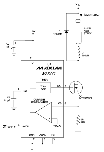
Figure 1. The connections shown convert this switch-mode voltage regulator to a general-purpose current source.
First, apply 5V to V+. Because the chip expects 12V of feedback at that terminal, it assumes a loss of regulation and shifts control to the current loop. This mode of operation allows an increasing ramp of current through Q1, causing the voltage at CS (pin 8) to increase until it reaches the internal comparator threshold (210mV). Timing circuitry then turns off Q1 for a fixed 2.3µs, and the cycle repeats. The result is a relatively constant inductor current, which is also the load current (Figure 2.)
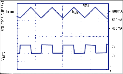
Figure 2. The gate drive for Q1 and the resulting current through L1 are related as shown.
With the proper component values, the circuit generates constant current over a wide range of input voltages. The Figure 1 circuit (with component values shown) is a fast charger for NiCd batteries that provides 600mA charging currents. Calculations are as follows:
The peak inductor current is IPEAK = VSENSE/R1, where VSENSE is the 210mV threshold of the current-sense comparator. The dither current (peak-to-peak value of the ac component of load current) is:
(1) IDITHER = VBATT tOFF/L,
where VBATT is the battery voltage, tOFF is the 2.3µs interval mentioned earlier, and L is the inductance of L1.
As illustrated in Figure 2, the average inductor current is IAVE = IPEAK - ½IDITHER. Substituting from above,

First, choose an average current for the proposed current source (600mA in this circuit). Next, determine the nominal value of VBATT (4.8V in this case). Next, to ensure a relatively small ac (vs. dc) component, set the dither current in equation 1 less than 0.2IAVE and solve for L:

(Use L = 100µH.)
Next, plug this L value (100µH) into equation 2 and solve for R1:

(Use R1 = 300mΩ.)
Three forms of error cause IAVE to deviate from the specified 600mA (Figure 3): variations in VSENSE, delay through the comparator and MOSFET (Q1), and tolerance on the current-sense resistor R1. At lower voltages, the largest error is that of VSENSE, specified in the IC1 data sheet as 210mV ±30mV or about 14%. (In this circuit the value was about 190mV.)
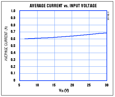
Figure 3. Current-source errors increase with input voltage, as explained in the text.
At higher voltages, delays cause the peak current to overshoot the current limit. You can minimize this error by choosing the inductor value as follows:
(5) L (in µH) > 5.5 (VIN VBATT),
with VIN and VBATT in volts.
Other error sources-the variations in VBATT, tOFF, and L-are relatively small because they relate to IDITHER, which is limited to a small fraction of IAVE.
打开APP阅读更多精彩内容
The switching regulator of Figure 1 includes independent loops of current and voltage feedback for maintaining regulation. By disabling the voltage loop, you can use the current loop to implement a general-purpose current source.

Figure 1. The connections shown convert this switch-mode voltage regulator to a general-purpose current source.
First, apply 5V to V+. Because the chip expects 12V of feedback at that terminal, it assumes a loss of regulation and shifts control to the current loop. This mode of operation allows an increasing ramp of current through Q1, causing the voltage at CS (pin 8) to increase until it reaches the internal comparator threshold (210mV). Timing circuitry then turns off Q1 for a fixed 2.3µs, and the cycle repeats. The result is a relatively constant inductor current, which is also the load current (Figure 2.)

Figure 2. The gate drive for Q1 and the resulting current through L1 are related as shown.
With the proper component values, the circuit generates constant current over a wide range of input voltages. The Figure 1 circuit (with component values shown) is a fast charger for NiCd batteries that provides 600mA charging currents. Calculations are as follows:
The peak inductor current is IPEAK = VSENSE/R1, where VSENSE is the 210mV threshold of the current-sense comparator. The dither current (peak-to-peak value of the ac component of load current) is:
(1) IDITHER = VBATT tOFF/L,
where VBATT is the battery voltage, tOFF is the 2.3µs interval mentioned earlier, and L is the inductance of L1.
As illustrated in Figure 2, the average inductor current is IAVE = IPEAK - ½IDITHER. Substituting from above,

First, choose an average current for the proposed current source (600mA in this circuit). Next, determine the nominal value of VBATT (4.8V in this case). Next, to ensure a relatively small ac (vs. dc) component, set the dither current in equation 1 less than 0.2IAVE and solve for L:

(Use L = 100µH.)
Next, plug this L value (100µH) into equation 2 and solve for R1:

(Use R1 = 300mΩ.)
Three forms of error cause IAVE to deviate from the specified 600mA (Figure 3): variations in VSENSE, delay through the comparator and MOSFET (Q1), and tolerance on the current-sense resistor R1. At lower voltages, the largest error is that of VSENSE, specified in the IC1 data sheet as 210mV ±30mV or about 14%. (In this circuit the value was about 190mV.)

Figure 3. Current-source errors increase with input voltage, as explained in the text.
At higher voltages, delays cause the peak current to overshoot the current limit. You can minimize this error by choosing the inductor value as follows:
(5) L (in µH) > 5.5 (VIN VBATT),
with VIN and VBATT in volts.
Other error sources-the variations in VBATT, tOFF, and L-are relatively small because they relate to IDITHER, which is limited to a small fraction of IAVE.
声明:本文内容及配图由入驻作者撰写或者入驻合作网站授权转载。文章观点仅代表作者本人,不代表电子发烧友网立场。文章及其配图仅供工程师学习之用,如有内容侵权或者其他违规问题,请联系本站处理。
举报投诉
- 相关推荐
- 热点推荐
- 电流源
-
降压型与升压型DC-DC转换器的输出纹波有什么不同2024-10-09 2188
-
什么是DC/DC转换器?2024-09-29 852
-
降压型DC-DC转换器与升压型DC-DC转换器的输出纹波差异2024-04-24 2832
-
Boost升压型DC-DC转换电路介绍2024-02-01 3896
-
DC-DC转换器电路图 Boost升压型DC-DC转换器的工作原理2023-09-19 5274
-
基于MAX1771 DC-DC控制器的开关模式电流源设计2023-03-17 1555
-
升压DC-DC稳压器转换为电流源进行电池充电2023-03-07 1886
-
Buck型DC-DC的相关资料分享2021-11-17 1399
-
非隔离式的DC-DC转换器解析2020-12-09 5492
-
PFM/PWM升压型DC/DC控制器2020-08-05 2944
-
Ap1603升压型DC-DC转换器的典型应用2020-06-19 2734
-
高效率的Ap1603升压型DC-DC转换器的应用2020-06-18 2637
-
在系统中成功运用DC-DC降压/升压调节器2018-11-01 2676
-
DC-DC降压/升压调节器设计方案2012-04-10 4997
全部0条评论

快来发表一下你的评论吧 !

