
检测和校准1 DS2760锂电池监测与保护器电路-Testi
电源新闻
20人已加入
描述
Abstract: This application note describes to the reader how to properly test a circuit board and battery pack containing a Dallas Semiconductor DS2760 battery monitor and protector. A step-by-step test procedure is provided which can be followed to ensure that the circuit boards and battery packs have been assembled properly. Additionally, this note also instructs the reader on how to properly calibrate the high-accuracy current A/D converter on the DS2760 battery monitor once it is assembled into a battery pack. Procedures for both the current offset and current gain calibrations are covered.

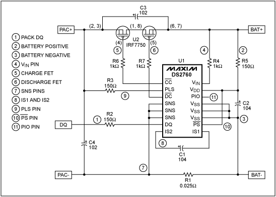
Figure 1. Circuit board nodes that must be verified.
Test 1: Test Initialization. The purpose of test initialization is to place the DS2760 registers into known states and determine there are any direct shorts on the board. Successful communication to the device in this step verifies the DQ connection (node 1) as well as Battery Positive to the VDD pin (node 2) and Battery Negative to the VSS pin and PAC- (node 3). The charge and discharge FETs are enabled then the Protection Register is checked for flag conditions:
Test 2: Verify VIN pin connection to Battery Positive (node 4). Read the latest voltage from the DS2760 and confirm it is a valid measurement:
Test 3: Operation of the Charge Control FET (node 5). Proper operation of the Charge Control FET can be verified by disabling the FET and attempting to force current into PAC+:
Test 4: Operation of the Discharge Control FET (node 6). Connections to the Discharge Control FET are verified by disabling the FET and attempting to force current out of PAC+:
Test 5: Verify SNS, IS1, and IS2 pin connections (nodes 7 and 8). Connections to the SNS pins can be verified easily with a valid current measurement. While validating the capacitor from IS1 to IS2 is difficult, a successful current measurement will prove they are not shorted to each other or to any of the surrounding pins:
Test 6: Verify PLS pin connection to Pack Positive (node 9). The PLS pin is used by the DS2760 to determine if an error condition is still present from PAC+ to PAC-. Force a discharge overcurrent condition and verify that the flag cannot be cleared, then remove the condition and verify that the flag can be cleared:
Test 7: Verify PS pin connection (node 10). If the PS pin is hardwired in the circuit, simply read the Special Feature Register (bit 7) to confirm the pin state. If the pin has an external connection to the board, toggle pin states and verify the change in the Special Feature Register:
Test 8: Verify PIO pin connection (node 11). If the PIO pin is being used as an input, perform a test similar to that of the PS pin above. If the pin is used as an output, toggle the pin in software while reading the bit back to verify its state:

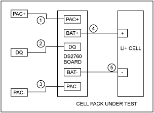
Figure 2. Cell pack nodes that must be verified.
Test 1: Communication. The simple act of reading the DS2760's net address verifies most of the connections in this circuit. For proper communication, the DQ pin (node 2) and PAC- (node 3) must be valid connections. For the DS2760 to properly respond, the board must be powered through BAT+ (node 4) and BAT- (node 5). The communication test is:
Test 2: Power. To verify that PAC+ is properly connected to the DS2760 board, enable the FETs and verify that the cell voltage can be measured on the PAC+ pin. Also check the DS2760 to see if any short circuits were detected:
Test 3: PIO and PS. If pack design uses the PIO and PS pins as inputs or outputs, verify their operation by toggling pin states and confirming the results in the Special Feature Register. See test steps 7 and 8 in the board level test section above.
The Current A/D offset should be calibrated after assembly into the pack. For greatest accuracy, multiple measurements should be made over the longest acceptable period of time while the control FETs are disabled guaranteeing no current flow in the system.
打开APP阅读更多精彩内容
Introduction
The advantages of lithium-ion protection and high accuracy fuel gauging can be completely negated by an assembly error or improper calibration of the device. This application notes walks through examples of how to test an assembled protection circuit board and a fully assembled pack followed by a step by step process to properly calibrate the DS2760's high accuracy Current A/D.Performing a Board Level Test
The following is an example of how to production test a DS2760 based protection circuit board before final assembly into a cell pack. Figure 1 shows a sample circuit board schematic utilizing all the DS2760's features. All critical test points (there are 11) are indicated with circled numbers in the figure. This test flow assumes all discrete components of the circuit have been tested and therefore the goal is to verify the board has been assembled properly by validating the connections.
Figure 1. Circuit board nodes that must be verified.
Test 1: Test Initialization. The purpose of test initialization is to place the DS2760 registers into known states and determine there are any direct shorts on the board. Successful communication to the device in this step verifies the DQ connection (node 1) as well as Battery Positive to the VDD pin (node 2) and Battery Negative to the VSS pin and PAC- (node 3). The charge and discharge FETs are enabled then the Protection Register is checked for flag conditions:
| Force 4.0V from BAT+ to BAT- | ||
| Write 0x00h to the Protection Register | Clear all flags | |
| Write 0x03h to the Protection Register | Enable FETs | |
| Wait 150 ms | Wait for test of all possible flag conditions | |
| Read the Protection Register | Read DOC flag | |
| Fail board if DOC Flag (bit 4) is set. | ||
| Fail board if communication is not possible. | ||
Test 2: Verify VIN pin connection to Battery Positive (node 4). Read the latest voltage from the DS2760 and confirm it is a valid measurement:
| Force 4.0V from BAT+ to BAT- | ||
| Wait 10 ms | Wait for voltage conversion | |
| Read Voltage Register | 2 Bytes | |
| Fail board if Voltage reading is inaccurate. | ||
Test 3: Operation of the Charge Control FET (node 5). Proper operation of the Charge Control FET can be verified by disabling the FET and attempting to force current into PAC+:
| Force 4.0V from BAT+ to BAT- | ||
| Attempt to force current into PAC+ | A minimum of 100mA is recommended | |
| Fail board if current cannot be forced | ||
| Write 0x01h to the Protection Register | Disable Charge FET | |
| Attempt to force current into PAC+ | A minimum of 1mA is recommended | |
| Fail board if current can be forced | ||
| Write 0x03h to the Protection Register | Enable Charge FET | |
Test 4: Operation of the Discharge Control FET (node 6). Connections to the Discharge Control FET are verified by disabling the FET and attempting to force current out of PAC+:
| Force 4.0V from BAT+ to BAT- | ||
| Attempt to force current out of PAC+ | A minimum of 100mA is recommended | |
| Fail board if current cannot be forced | ||
| Write 0x02h to the Protection Register | Disable Discharge FET | |
| Attempt to force current out of PAC+ | A minimum of 1mA is recommended | |
| Fail board if current can be forced | ||
| Write 0x03h to the Protection Register | Enable Discharge FET | |
Test 5: Verify SNS, IS1, and IS2 pin connections (nodes 7 and 8). Connections to the SNS pins can be verified easily with a valid current measurement. While validating the capacitor from IS1 to IS2 is difficult, a successful current measurement will prove they are not shorted to each other or to any of the surrounding pins:
| Force 4.0V from BAT+ to BAT- | ||
| Force 1.0A out of PAC+ | ||
| Wait 100 ms | Wait for current conversion | |
| Read Current Register | 2 Bytes | |
| Fail board if Current reading is inaccurate | ||
Test 6: Verify PLS pin connection to Pack Positive (node 9). The PLS pin is used by the DS2760 to determine if an error condition is still present from PAC+ to PAC-. Force a discharge overcurrent condition and verify that the flag cannot be cleared, then remove the condition and verify that the flag can be cleared:
| Force 4.0V from BAT+ to BAT- | ||
| Force 2.5A out of PAC+ | ||
| Wait 20 ms | Wait for condition to update flags | |
| Write 0x00h to the Protection Register | Attempt to clear all flags | |
| Read the Protection Register | Read DOC flag | |
| Fail board if DOC Flag is clear | ||
| Force 0.0A out of PAC+ | ||
| Wait 20 ms | Wait for condition to update flags | |
| Write 0x00h to the Protection Register | Clear all flags | |
| Read the Protection Register | Read DOC flag | |
| Fail board if DOC Flag is set | ||
Test 7: Verify PS pin connection (node 10). If the PS pin is hardwired in the circuit, simply read the Special Feature Register (bit 7) to confirm the pin state. If the pin has an external connection to the board, toggle pin states and verify the change in the Special Feature Register:
| Force 4.0V from BAT+ to BAT- | ||
| Force PS pin low externally | ||
| Read the Special Feature Register | Read PS pin state | |
| Fail board if PS bit is set | ||
| Force PS pin high externally | ||
| Read the Special Feature Register | Read PS pin state | |
| Fail board if PS bit is cleared | ||
Test 8: Verify PIO pin connection (node 11). If the PIO pin is being used as an input, perform a test similar to that of the PS pin above. If the pin is used as an output, toggle the pin in software while reading the bit back to verify its state:
| Force 4.0V from BAT+ to BAT- | ||
| Write 0x00 to the Special Feature Register | Force PIO pin low | |
| Read the Special Feature Register | Read PIO pin state | |
| Fail board if PIO bit is set | ||
| Write 0x40 to the Special Feature Register | Force PIO pin high | |
| Read the Special Feature Register | Read PIO pin state | |
| Fail board if PIO bit is cleared | ||
Performing a Pack Level Test
Performing a test on the assembled pack is more straightforward than the board level test above. This example test flow assumes the DS2760 based protection circuit board and lithium-ion cell have each been individually verified prior to pack assembly and the cell has sufficient charge to power the protection board. The example cell pack is shown in Figure 2. All critical test nodes are indicated with a circled number.
Figure 2. Cell pack nodes that must be verified.
Test 1: Communication. The simple act of reading the DS2760's net address verifies most of the connections in this circuit. For proper communication, the DQ pin (node 2) and PAC- (node 3) must be valid connections. For the DS2760 to properly respond, the board must be powered through BAT+ (node 4) and BAT- (node 5). The communication test is:
| Read the Net Address | ||
| Fail pack if communication is not possible. | ||
Test 2: Power. To verify that PAC+ is properly connected to the DS2760 board, enable the FETs and verify that the cell voltage can be measured on the PAC+ pin. Also check the DS2760 to see if any short circuits were detected:
| Write 0x00h to the Protection Register | Clear all flags | |
| Write 0x03h to the Protection Register | Enable FETs | |
| Wait 150ms | Wait for test of all possible flag conditions | |
| Read the Protection Register | Read DOC flag | |
| Fail pack if DOC Flag (bit 4) is set. | ||
| Fail pack if cell voltage cannot be measured at PAC+ | ||
Test 3: PIO and PS. If pack design uses the PIO and PS pins as inputs or outputs, verify their operation by toggling pin states and confirming the results in the Special Feature Register. See test steps 7 and 8 in the board level test section above.
Calibrating the Current Offset
The current A/D of the DS2760 is extremely sensitive. It is capable of measuring a voltage drop of only 15µV across the sense resistor. This kind of accuracy can only be achieved by calibrating the current measurement after the cell pack is assembled. The current offset register allows the current measurements of the DS2760 to be adjusted by ±127 LSbs for accurate measurement of very small currents. The following example lists the steps to calibrate the DS2760 in circuit:- Write 0x00 to the Protection Register to disable all charging and discharging.
- Average 32 current measurements with at least a 100 ms interval between samples. It is recommended to use many readings as possible for best accuracy.
- If the averaged current register value is greater than ±127 LSbs (±79.375mA or ±1.984mV) the device cannot be trimmed to zero. Verify circuit.
- Store the resulting value in the Current Offset Register location 0x33h and copy to EEPROM.
- Verify accuracy with additional current measurements. Repeat process if necessary.
Calibrating the Current Gain
DS2760s with integrated sense resistors are calibrated at the factory to accurately report current, no further calibration is necessary. The DS2760 without integrated sense resistor will be factory calibrated to measure voltage. To accurately convert this voltage value into a current reading, the exact sense resistance must be known. Dallas Semiconductor recommends measuring this resistance at pack assembly and storing the value in EEPROM for reference by the handset. A sample procedure for this process would be as follows:- Accurately measure the sense resistance of the assembled circuit. This can be accomplished by forcing a known current through the pack and using the DS2760 to measure the voltage drop across the sense resistor.
- Store the resistance value in unused DS2760 EEPROM. Dallas Semiconductor recommends storing with at least
0.25mΩ resolution. One byte would provide a range of 0mΩ to 63.75mΩ. - During operation, the handset reads this resistance value and multiplies the Current Register and Current Accumulator values with it to calculate the measured current and accumulated charge.
Summary
Proper verification of an assembled DS2760 based lithium-ion cell pack requires testing of every solder point in the circuit. At the very minimum, the test should verify that the protection prevents all current flow into and out of the pack when the control FETs are disabled.The Current A/D offset should be calibrated after assembly into the pack. For greatest accuracy, multiple measurements should be made over the longest acceptable period of time while the control FETs are disabled guaranteeing no current flow in the system.
声明:本文内容及配图由入驻作者撰写或者入驻合作网站授权转载。文章观点仅代表作者本人,不代表电子发烧友网立场。文章及其配图仅供工程师学习之用,如有内容侵权或者其他违规问题,请联系本站处理。
举报投诉
- 相关推荐
- 热点推荐
- DS2760
-
锂电池保护器和电池的区别2024-10-17 1884
-
测试和校准DS2760锂离子电池监测和保护器电路2023-03-09 1665
-
DS2760 1-Wire高精度锂离子电池监视和保护IC在微控制器环境中的接口2023-03-01 2058
-
DS2760或DS2761电池监测器在多节电池中的应用2023-01-11 2421
-
DS2762高精度锂电池监测集成电路相关资料分享2021-05-18 1320
-
【浩博电池资讯】8大保护锂电池的保护板2019-08-01 4841
-
请问怎么检测锂电池保护板?2018-07-16 8241
-
锂电池监测芯片2014-05-23 2039
-
多种电池组应用的DS2760或DS2761-Multiple2009-04-30 1843
-
Interfacing the DS2760 1-Wire2009-04-23 1538
-
锂离子电池保护器及监控器 (图)2008-09-12 5186
全部0条评论

快来发表一下你的评论吧 !

