

Reference Design for a High-Cu
新品快讯
29人已加入
描述
|
Reference Design for a High-Current Power Supply with Lossless Current Sensing Using the MAX5060 abstract: This reference design shows how to use a MAX5060 current-mode, step-down power-supply controller to implement lossless current sensing for high-current applications. In this design, the series resistance (DCR) of the inductor is used for current sensing to avoid power loss in the current-sense resistor. IntroductionToday's data processing elements demand higher currents from power supplies to achieve higher speed. Lossless current sensing and ground bouncing are key challenges for accurate control of output voltage and current in these applications.The MAX5060 PWM buck power-supply controller uses an average-current-mode control technique to track the load current, and it employs differential sensing to accurately control the output voltage. In this reference design, the series resistance (DCR) of the inductor is used for current sensing to avoid power loss in the current-sense resistor. This design shows a solution for implementing a high-current (30A) power supply with high system efficiency and good load regulation. The complete schematic, bill of materials (BOM), efficiency measurements, and test results are included below. Specifications and Design SetupThis reference design achieves the following specifications.Input Voltage: 12V ±10% Output Voltage: 1.5V Output Current: 30A Output Ripple: ±15mV Input Ripple: ±250mV Efficiency: > 88% with Half of Full Load (15A) Switching Frequency: 275kHz Footprint Size: 5cm × 3.3cm The schematic for this reference design is shown in Figure 1, and the BOM is given in Table 1. In this design, the MAX5060 is used in a buck configuration. 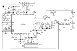 More detailed image (PDF, 100kB) Figure 1. Schematic of the MAX5060 buck converter for FSW = 275kHz. Table 1. Bill of Materials
Efficiency PlotsFigure 2 provides a plot of efficiency versus load current plots for this design, and Figure 3 presents load-regulation data.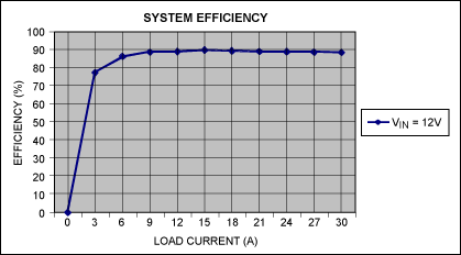 Figure 2. Load current versus converter efficiency for VIN = 12V. 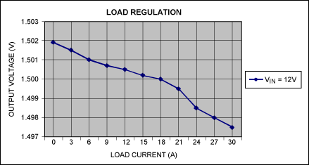 Figure 3. Load current versus converter output voltage for VIN = 12V. Experimental ResultsConverter output voltage and load current are shown in Figures 4–7 for different input excitations.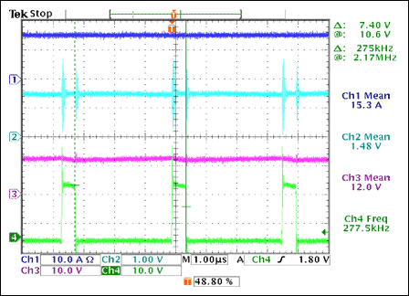 Figure 4. Converter waveforms with VIN = 12V and IOUT = 30A. VIN = 12V and IOUT = 2 × 15A Ch1: Output Current (2x) Ch2: Output Voltage Ch3: Input Voltage Ch4: High-Side MOSFET Gate Drive 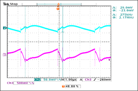 Figure 5. Input and output ripple waveforms with VIN = 12V and IOUT = 30A. VIN = 12V and IOUT = 2 × 15A Ch2: Output Voltage Ripple Ch3: Input Voltage Ripple 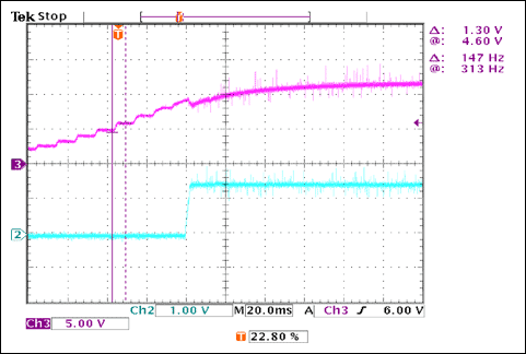 Figure 6. Line transient response. VIN = 0 to 12V and IOUT = 2 × 15A Ch2: Output Voltage Ch3: Input Voltage 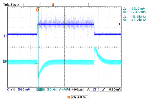 Figure 7. Load transient response. VIN = 12V and IOUT = 1A to 7A Ch1: Output Current Transient (1A to 7A) Ch2: Output Voltage Ripple The board developed for this application is shown in Figure 8. |
声明:本文内容及配图由入驻作者撰写或者入驻合作网站授权转载。文章观点仅代表作者本人,不代表电子发烧友网立场。文章及其配图仅供工程师学习之用,如有内容侵权或者其他违规问题,请联系本站处理。
举报投诉
-
432W High-Efficiency Single-Phase Synchronous Buck Converter Reference Design2015-04-15 2248
-
Reference Design for a High-In2009-11-08 1695
-
LED Reference Design Kit2009-10-23 735
-
Reference Design for a PC-Base2009-09-27 1159
-
Reference Design for a Signal-2009-06-30 1340
-
Reference Design Report for a2009-06-28 662
-
Reference Design for Power-ove2009-04-23 1453
-
Reference Design Ensures Dynam2009-03-23 1188
-
Reference Design for a Class-D2009-03-02 2231
-
WLAN Reference Design with the2009-02-22 1298
-
MAX1886 pdf datasheet (High-Cu2009-01-11 1334
-
WiBro Reference Design with th2008-09-17 1353
-
Transmitter Reference Design f2008-08-18 1333
全部0条评论

快来发表一下你的评论吧 !

