

新增高电压能力的MAX471/MAX472高侧电流检测放大器
电源设计应用
456人已加入
描述
Abstract: An avalanche diode and current source provide a floating power supply to allow high-side current sense amplifiers to work at up to 300V.
The MAX471 and MAX472 are complete bi-directional high-side current sense amplifiers for portable PCs, telephones, and other systems where battery/DC line monitoring is important, and where ground continuity between system and supply is crucial.
However, the part's 36V maximum operating voltage is a limiting factor when higher voltage systems are to be monitored, such as traction motor batteries and telecom central exchange power supplies, both of which require operation above 72V. New high-side current sense amplifiers such as the MAX4080, can operate up to 76V.
The circuit of Figure 1 shows a simple way to add high voltage capability to the basic MAX471/2. Low supply current of the current monitor (100µA) allows a very simple floating power supply formed by avalanche diode D1, C1, C2, and the NPN current source Q1 and Q2. The voltage compliance of the current source provides the high voltage capability. With the part shown, Motorola MPSA42 (Q1), 300V is the maximum recommended, giving an absolute maximum input voltage rating for the whole circuit of 305.1V. Use of a 33V avalanche diode for D1 pushes this to 333V.
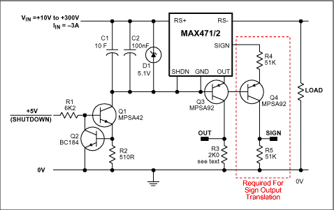
Figure 1. High voltage MAX471/2.
The OUT pin of the MAX471/2 is a current source of 500µA/A, whose output impedance is typically 3MΩ. A PNP common base stage, Q3, provides the high voltage compliance while retaining the ground reference capability of the output. An MPSA92 is complimentary to the MPSA42 and provides a matching 300V operation. Collector resistor R3 may be chosen to provide a particular full scale output voltage. With the prototype values chosen, the output voltage at Q3 collector changed by <10mV for an input voltage range of +10V to +300V.
A simple two transistor current source, Q1 and Q2, is accurate enough and is sufficient to provide voltage compliance and diode current. Chose the current value to ensure that the avalanche diode is regulating. 1mA was chosen for the prototype. The voltage supply to R1 biases the current source, and provides a suitable ground referenced point with which to switch off the whole circuit.
The common base stage Q3 allows the same scaling factors, as calculated for the MAX471/2, to be used at the collector with little additional error loss. Remember that the current gain for a common base stage is α, and is <1. Its value may be obtained from the DC β-spec in the transistor data sheet, namely
The MAX471/2 have a polarity output, which signals the direction of the current through the sense terminals. Adding Q4, another common base PNP stage adds high voltage compliance, and produces a ground referenced logic level output.
打开APP阅读更多精彩内容
The MAX471 and MAX472 are complete bi-directional high-side current sense amplifiers for portable PCs, telephones, and other systems where battery/DC line monitoring is important, and where ground continuity between system and supply is crucial.
However, the part's 36V maximum operating voltage is a limiting factor when higher voltage systems are to be monitored, such as traction motor batteries and telecom central exchange power supplies, both of which require operation above 72V. New high-side current sense amplifiers such as the MAX4080, can operate up to 76V.
The circuit of Figure 1 shows a simple way to add high voltage capability to the basic MAX471/2. Low supply current of the current monitor (100µA) allows a very simple floating power supply formed by avalanche diode D1, C1, C2, and the NPN current source Q1 and Q2. The voltage compliance of the current source provides the high voltage capability. With the part shown, Motorola MPSA42 (Q1), 300V is the maximum recommended, giving an absolute maximum input voltage rating for the whole circuit of 305.1V. Use of a 33V avalanche diode for D1 pushes this to 333V.
Figure 1. High voltage MAX471/2.
The OUT pin of the MAX471/2 is a current source of 500µA/A, whose output impedance is typically 3MΩ. A PNP common base stage, Q3, provides the high voltage compliance while retaining the ground reference capability of the output. An MPSA92 is complimentary to the MPSA42 and provides a matching 300V operation. Collector resistor R3 may be chosen to provide a particular full scale output voltage. With the prototype values chosen, the output voltage at Q3 collector changed by <10mV for an input voltage range of +10V to +300V.
A simple two transistor current source, Q1 and Q2, is accurate enough and is sufficient to provide voltage compliance and diode current. Chose the current value to ensure that the avalanche diode is regulating. 1mA was chosen for the prototype. The voltage supply to R1 biases the current source, and provides a suitable ground referenced point with which to switch off the whole circuit.
The common base stage Q3 allows the same scaling factors, as calculated for the MAX471/2, to be used at the collector with little additional error loss. Remember that the current gain for a common base stage is α, and is <1. Its value may be obtained from the DC β-spec in the transistor data sheet, namely
For the MPSA92, β(min) = 25, giving a figure for α(min) = 0.96. This can be improved by increasing the current gain of Q3, either with a Darlington or compound transistor connection.= β / (1 + β)
The MAX471/2 have a polarity output, which signals the direction of the current through the sense terminals. Adding Q4, another common base PNP stage adds high voltage compliance, and produces a ground referenced logic level output.
声明:本文内容及配图由入驻作者撰写或者入驻合作网站授权转载。文章观点仅代表作者本人,不代表电子发烧友网立场。文章及其配图仅供工程师学习之用,如有内容侵权或者其他违规问题,请联系本站处理。
举报投诉
- 相关推荐
- 热点推荐
- MAX471
-
MAX4376/MAX4377/MAX4378:高侧电流检测放大器的理想之选2026-01-14 513
-
探索MAX9611/MAX9612:高侧电流检测放大器的卓越之选2026-01-13 664
-
MAX471电流检测放大器的主要特性有哪些2021-10-15 2127
-
有人用过MAX471电流检测芯片吗?2020-08-10 3120
-
MAX471电流检测2020-05-30 1600
-
请教大神们,请问如何扩展MAX471电流检测的量程?2017-09-05 4191
-
MAX471 电流灵敏IC防止过流损坏2016-08-18 966
-
MAX471检测电流和真实电流相差很大,谁能告诉我是哪里的问题吗?2016-03-04 18475
-
MAX系列电流检测芯片2011-02-19 7723
-
MAX471/MAX472的特点、功能2009-07-02 3199
-
新增高电压能力的MAX471/MAX472高侧电流检测放大器2009-05-06 2128
-
MAX471/MAX472中文资料pdf2008-07-21 4232
全部0条评论

快来发表一下你的评论吧 !
