

3.3V Supply Taps Power from th
电源设计应用
454人已加入
描述
Additional Information:
The figure below shows a circuit that derives 3.3V from -12V by boosting the -12V supply to 15.3V (with respect to the -12V rail) and provides up to 300mA. Transistor Q2 level-shifts the 3.3V output to the feedback level of -10.75V.
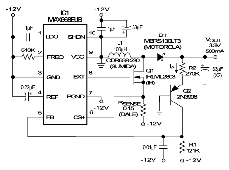
This PWM boost-controller IC provides relief to an overloaded 3.3V backplane supply by generating a supplemental 3.3V regulated output from the lightly loaded -12V rail of a VME, VXI, or PCI backplane.
The circuit occupies approximately 6.25cm² of PC-board space and employs a PWM boost controller that delivers 1W at 83% efficiency levels.
Because the sense resistor (RSENSE) limits peak currents to about 120mA, the n-channel switching MOSFET (Q1) can be an inexpensive logic-level device. Resistors R1 and R2 permit selection of VOUT to either 3.3V or 5V.
Note that the feedback voltage at equilibrium (pin 5, as determined by the trip point of a comparator internal to IC1) is 1.25V above the PGND terminal (pin 7). To calculate the appropriate R1/R2 values:
The circuit is optimized for a 1W output in applications associated with desktop-PC power supplies. In these applications, efficiency must exceed 83%, because the -12V bus is power-limited to 1.2W. If necessary, the output power can be increased to 3W (3V at 1A or more) by scaling L1, D1, and RSENSE. A diode can be added in series with R1 to block unwanted reverse currents.
A similar version of this article appeared in the February 7, 2000 issue of Electronic Design.
打开APP阅读更多精彩内容
- Quick View Data Sheet for the MAX668
- Samples and Literature Order Form
- Technical Support: Power
The figure below shows a circuit that derives 3.3V from -12V by boosting the -12V supply to 15.3V (with respect to the -12V rail) and provides up to 300mA. Transistor Q2 level-shifts the 3.3V output to the feedback level of -10.75V.
This PWM boost-controller IC provides relief to an overloaded 3.3V backplane supply by generating a supplemental 3.3V regulated output from the lightly loaded -12V rail of a VME, VXI, or PCI backplane.
The circuit occupies approximately 6.25cm² of PC-board space and employs a PWM boost controller that delivers 1W at 83% efficiency levels.
Because the sense resistor (RSENSE) limits peak currents to about 120mA, the n-channel switching MOSFET (Q1) can be an inexpensive logic-level device. Resistors R1 and R2 permit selection of VOUT to either 3.3V or 5V.
Note that the feedback voltage at equilibrium (pin 5, as determined by the trip point of a comparator internal to IC1) is 1.25V above the PGND terminal (pin 7). To calculate the appropriate R1/R2 values:
VFB = -12V + 1.25V = -10.75VChoosing an arbitrary value for R1:
I2 = 1.25V/R1 = 1.25V/12.1k = 103µATherefore,
R2 = (VOUT - VBE)/I2 = (3.3V - 0.7V)/103µA = 25.2kIC1 has another capability that is useful in RF applications, DAQ modules, and other noise-sensitive designs: It lets you program the switching frequency between 100kHz and 500kHz using an external resistor. The circuit's high frequency (100kHz) maintains high efficiency while allowing the use of small inductor and capacitor values.
The circuit is optimized for a 1W output in applications associated with desktop-PC power supplies. In these applications, efficiency must exceed 83%, because the -12V bus is power-limited to 1.2W. If necessary, the output power can be increased to 3W (3V at 1A or more) by scaling L1, D1, and RSENSE. A diode can be added in series with R1 to block unwanted reverse currents.
A similar version of this article appeared in the February 7, 2000 issue of Electronic Design.
声明:本文内容及配图由入驻作者撰写或者入驻合作网站授权转载。文章观点仅代表作者本人,不代表电子发烧友网立场。文章及其配图仅供工程师学习之用,如有内容侵权或者其他违规问题,请联系本站处理。
举报投诉
- 相关推荐
- 热点推荐
- PCI
-
LT3066 Demo Circuit - 3.3V Supply with 497mA Precision Current Limit (3.6-45V to 3.3V @ 450mA)2021-03-11 716
-
高效率5V至3.3V 1.2A DC-DC转换器包括BOM及层图2018-09-21 2678
-
2W 88-269VAC 输入、+3.3V 和 -3.3V 双输出参考设计2015-03-12 2308
-
Riverside (MAXREFDES8#)3.3V Input, 12V (15V) Output Isolated Power Supply2012-11-07 629
-
PT6913,pdf(12 Watt 5V/3.3V Inp2010-11-18 844
-
PT6914,pdf(12 Watt 5V/3.3V Inp2010-11-16 873
-
3.3V DSP for Digital Motor Con2009-11-12 532
-
DS90LV019,pdf datasheet (3.3V2009-10-13 783
-
ADN2880: 3.2 Gbps 3.3V Low No2009-09-23 1604
-
Isolated SLIC Supply2009-05-04 1300
-
电力保护3V/5V双电源系统-Power Conservat2009-04-29 1688
-
3.3V, HD Video Filter Amplifie2008-12-10 1690
全部0条评论

快来发表一下你的评论吧 !
