

保护电流检测放大器反对过压瞬变-Protect Curren
电源设计应用
454人已加入
描述
Abstract: This application note describes methods of protecting lower-voltage current sense amplifiers from high-voltage spikes and transients. Such conditions are frequently encountered in automotive car battery operation, and are referred to as load-dump conditions.
A similar article appeared in the October 25, 2007 issue of Electronic Design.
Some current-sense amplifiers encounter overvoltages frequently. A current-sense amplifier that monitors battery-discharge currents in an automobile, for example, must withstand the high-voltage load-dump pulses produced when loads are disconnected from the battery, causing inductive spikes and overvoltages to appear at the output of the alternator. If these pulses exceed the amplifier's common-mode voltage, then one must provide external circuitry to protect the amplifier.
Figure 1 shows an example of a protection circuit, which is composed of zener diodes Z1 and Z2, resistors R1 and R2, and diode D1. The common-mode voltage range of the MAX4372 amplifier is 0 to 28V, which is more than sufficient for measuring automotive battery voltages that vary from 6V to 18V. Load-dump voltages, however, can reach 35V and persist for 0.5 seconds, which is well over the amplifier's 30V absolute maximum rating for input voltage. The amplifier must therefore be well-protected externally.
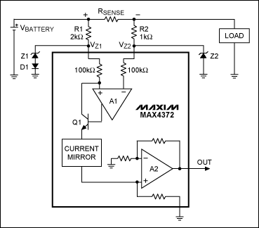
Figure 1. This current-sense amplifier has protection circuitry (upper circuit components) suitable for common-mode voltages above 30V.
You can avoid additional errors in the input offset voltage by using different values for the input-protection resistors R1 and R2 (2kΩ and 1kΩ, respectively), thereby balancing the effect of the amplifier's unequal bias currents. For selection of these resistor values, refer to the application note 3888, "Performance of Current-Sense Amplifiers with Input Series Resistors."
Zener diodes Z1 and Z2 have nominal breakdown voltage of 24V, and are chosen to have sufficient power-dissipation capability to withstand the ~11mA sink currents that flow during a 35V peak load-dump condition (the 35V load-dump voltage minus a 24V clamp voltage appears across the 1kΩ series resistor R2).
Figure 2 depicts the amplifier output in the presence of 35V load-dump pulses with D1 removed. With normal battery voltages applied, the 1V output value is as expected (input VSENSE = 50mV, and gain = 20). When a load-dump voltage appears, the zeners clamp the input common-mode voltage to about 24V, and the amplifier output makes a few transient excursions before settling down to 0V.
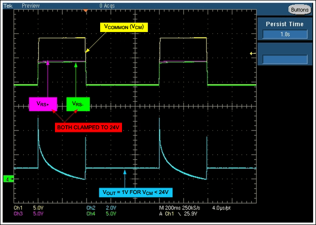 Figure 2. Operation of the Figure 1 circuit with diode D1 removed.
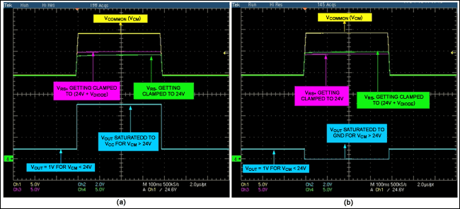
Though nominally 24V, the two zeners generally have slightly different breakdown voltages due to part-to-part variations and different operating currents (Z1 operates at 5.5mA and Z2 operates at 11mA). Therefore, the quantity (VZ1 - VZ2) appears as a changing differential sense voltage causing unwanted output transients. If desired, you can eliminate these transients by adding a diode in series with either Z1 or Z2. The diode forces (VZ1 - VZ2) to be either positive or negative during a load-dump condition, which in turn forces the amplifier output to one of the supply rails (VCC or GND), and thereby preventing random output response during an input transient.
Figure 3a shows the circuit operating with the diode connected in series with Z1, which forces the amplifier output to the positive rail. Figure 3b shows the diode connected in series with Z2, which forces the amplifier output to the negative rail.
More detailed image (PDF, 892kB)
Figure 3. Operation of the Figure 1 circuit with D1 in series with Z1 (a), and D1 in series with Z2 (b).
打开APP阅读更多精彩内容
A similar article appeared in the October 25, 2007 issue of Electronic Design.
Some current-sense amplifiers encounter overvoltages frequently. A current-sense amplifier that monitors battery-discharge currents in an automobile, for example, must withstand the high-voltage load-dump pulses produced when loads are disconnected from the battery, causing inductive spikes and overvoltages to appear at the output of the alternator. If these pulses exceed the amplifier's common-mode voltage, then one must provide external circuitry to protect the amplifier.
Figure 1 shows an example of a protection circuit, which is composed of zener diodes Z1 and Z2, resistors R1 and R2, and diode D1. The common-mode voltage range of the MAX4372 amplifier is 0 to 28V, which is more than sufficient for measuring automotive battery voltages that vary from 6V to 18V. Load-dump voltages, however, can reach 35V and persist for 0.5 seconds, which is well over the amplifier's 30V absolute maximum rating for input voltage. The amplifier must therefore be well-protected externally.
Figure 1. This current-sense amplifier has protection circuitry (upper circuit components) suitable for common-mode voltages above 30V.
You can avoid additional errors in the input offset voltage by using different values for the input-protection resistors R1 and R2 (2kΩ and 1kΩ, respectively), thereby balancing the effect of the amplifier's unequal bias currents. For selection of these resistor values, refer to the application note 3888, "Performance of Current-Sense Amplifiers with Input Series Resistors."
Zener diodes Z1 and Z2 have nominal breakdown voltage of 24V, and are chosen to have sufficient power-dissipation capability to withstand the ~11mA sink currents that flow during a 35V peak load-dump condition (the 35V load-dump voltage minus a 24V clamp voltage appears across the 1kΩ series resistor R2).
Figure 2 depicts the amplifier output in the presence of 35V load-dump pulses with D1 removed. With normal battery voltages applied, the 1V output value is as expected (input VSENSE = 50mV, and gain = 20). When a load-dump voltage appears, the zeners clamp the input common-mode voltage to about 24V, and the amplifier output makes a few transient excursions before settling down to 0V.
Figure 2. Operation of the Figure 1 circuit with diode D1 removed.Though nominally 24V, the two zeners generally have slightly different breakdown voltages due to part-to-part variations and different operating currents (Z1 operates at 5.5mA and Z2 operates at 11mA). Therefore, the quantity (VZ1 - VZ2) appears as a changing differential sense voltage causing unwanted output transients. If desired, you can eliminate these transients by adding a diode in series with either Z1 or Z2. The diode forces (VZ1 - VZ2) to be either positive or negative during a load-dump condition, which in turn forces the amplifier output to one of the supply rails (VCC or GND), and thereby preventing random output response during an input transient.
Figure 3a shows the circuit operating with the diode connected in series with Z1, which forces the amplifier output to the positive rail. Figure 3b shows the diode connected in series with Z2, which forces the amplifier output to the negative rail.
More detailed image (PDF, 892kB)
Figure 3. Operation of the Figure 1 circuit with D1 in series with Z1 (a), and D1 in series with Z2 (b).
声明:本文内容及配图由入驻作者撰写或者入驻合作网站授权转载。文章观点仅代表作者本人,不代表电子发烧友网立场。文章及其配图仅供工程师学习之用,如有内容侵权或者其他违规问题,请联系本站处理。
举报投诉
-
仪表放大器和电流检测放大器的区别2024-09-20 561
-
电流检测放大器的 差分过压保护电路2024-01-05 1611
-
电流检测放大器的差分过压保护电路分析2023-04-30 1439
-
保护电流检测放大器免受负过压影响2023-01-14 3407
-
模拟输入高压瞬变浪涌保护ESD保护二极管2021-11-23 1009
-
差动放大器和电流检测放大器2018-11-05 2599
-
电流检测放大器的差分过压保护电路2018-11-01 2431
-
电流检测放大器的远程电流检测配置2018-10-30 2879
-
电流检测放大器简介及其差分过压保护电路2017-09-12 1511
-
鲁棒的放大器提供集成过压保护2012-11-02 1962
-
瞬变电流检测仪原理图2012-04-26 7425
-
检流放大器的瞬态过压保护2009-07-18 1014
-
保护电流检测放大器反对过压瞬变-Protect Curren2009-05-02 760
-
反对数放大器2009-04-09 1476
全部0条评论

快来发表一下你的评论吧 !
