

Extend Current-Sense Amplifier
电源设计应用
455人已加入
描述
Abstract: Adding a charge pump provides ±5V supply rails to the operational amplifier internal to a high-side current-sense amplifier. This modification enables that amplifier to sense currents down to 0V common-mode inputs. The circuit can be modified to accommodate bidirectional current-sense applications.
In addition to the traditional lead-acid battery, modern electric/hybrid cars often include a large capacitor of 40 farads or more as a backup power source. Located under the rear seat, the large capacitor is used as a backup power supply to power the electronic braking system to safely stop the vehicle in case of engine and battery failure. Lead-acid batteries discharge only down to about 8V, but a capacitor can discharge down to 0V. Therefore, a current-sense amplifier is needed that can measure inputs down to 0V.
Most high-side current-sense amplifiers operate over a limited range of common-mode input and supply voltages. Consider, for example, the MAX4081, whose common-mode input and supply voltages range from 76V to 4.5V. To set the zero load-current point (the voltage output corresponding to zero load current, where VSENSE = 0V) for a bidirectional (charge/discharge) current-sensing application, one normally connects an external reference (+2.5V, for example) to the reference input (REF). For the MAX4081, however, the lower common-mode limit of 4.5V prohibits its use in applications that require current sensing close to ground.
This problem can be solved by connecting a charge pump to the circuit (Figure 1). The tiny charge pump (IC2) is powered from +5V, as is the current-sense amplifier. The output of the charge pump (-5V) acts as a negative supply voltage at the "GND" pin of IC1. REFA and REFB are connected to circuit Ground.
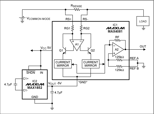
Figure 1. Adding a -5V rail to this current-sense amplifier extends its lower common-mode limit from 4.5V to 0V.
The internal op amp (A2) of IC1 now operates from ±5V rails (a 10V span), with its noninverting input (REF pins) sitting at the 0V midrail level. For VSENSE = 0V, the output voltage is 0V. VSENSE then increases with load current, producing an output of 5x, 20x, or 60x, according to the part number's gain suffix F, T, or S. The effective common-mode range now extends from 0V to +70V, with the original specifications unchanged (VOS < 0.6mV, and gain error < 0.6%).
You can also configure this circuit for bidirectional current-sense applications that operate from a single supply voltage (Figure 2). The ADC reference output drives the REFA pin to set the zero load-current point for IC1. For the gain option of 20V/V, for example, if the ADC reference voltage is +5V, the OUT to the ADC will be +2.5V at the zero load current. When current is flowing from battery to the load, the VSENSE can increase from 0V to +100mV and the OUT voltage will increase by +2.0V to +4.5V. If the same large current is flowing in the opposite direction (charging the battery), OUT will decrease from its zero current level by -2V, thus from 2.5V to 0.5V to monitor bidirectional currents using a 0V to 5V ADC input.
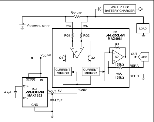
Figure 2. Connecting the reference voltage from an ADC to the current-sense amplifier lets the circuit monitor bidirectional currents.
Test results for the Figure 1 circuit (Figures 3 and 4) show that the current-sense amplifier's common-mode voltage (with GND connected to -5V) goes down to -2.8V. In contrast, common-mode voltage for the standard application (with GND connected to 0V) goes down only to +2.3V. With the -5V charge pump at the "GND" pin and with REFA and REFB connected to circuit GND, however, the output can swing nearly ±5V and below circuit GND.
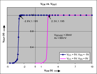
Figure 3. As shown in this plot of the Figure 1 output voltage, the addition of a charge pump extends IC1's common-mode range to 2.8V below ground.
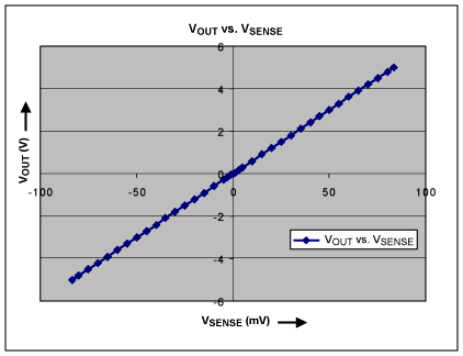
Figure 4. For IC1 in Figures 1 and 2, operating with a gain of 60V/V and a common-mode voltage of 0V, VOUT vs. VSENSE is linear over the entire VSENSE range (-80mV to +80mV).
The typical supply current of IC1 (103µA) presents a small load current to IC2, which prevents overloading and voltage drooping at its output. Take care when the output moves below GND. Load current then flows out of IC1's GND terminal and into the charge pump, whose negative output can droop as a result (rise toward 0V). As a countermeasure, you can use bigger capacitors in the charge pump or restrict the sense amplifier's output voltage.
A similar article appeared in the February 15, 2007 issue of Electronic Design magazine.
打开APP阅读更多精彩内容
In addition to the traditional lead-acid battery, modern electric/hybrid cars often include a large capacitor of 40 farads or more as a backup power source. Located under the rear seat, the large capacitor is used as a backup power supply to power the electronic braking system to safely stop the vehicle in case of engine and battery failure. Lead-acid batteries discharge only down to about 8V, but a capacitor can discharge down to 0V. Therefore, a current-sense amplifier is needed that can measure inputs down to 0V.
Most high-side current-sense amplifiers operate over a limited range of common-mode input and supply voltages. Consider, for example, the MAX4081, whose common-mode input and supply voltages range from 76V to 4.5V. To set the zero load-current point (the voltage output corresponding to zero load current, where VSENSE = 0V) for a bidirectional (charge/discharge) current-sensing application, one normally connects an external reference (+2.5V, for example) to the reference input (REF). For the MAX4081, however, the lower common-mode limit of 4.5V prohibits its use in applications that require current sensing close to ground.
This problem can be solved by connecting a charge pump to the circuit (Figure 1). The tiny charge pump (IC2) is powered from +5V, as is the current-sense amplifier. The output of the charge pump (-5V) acts as a negative supply voltage at the "GND" pin of IC1. REFA and REFB are connected to circuit Ground.

Figure 1. Adding a -5V rail to this current-sense amplifier extends its lower common-mode limit from 4.5V to 0V.
The internal op amp (A2) of IC1 now operates from ±5V rails (a 10V span), with its noninverting input (REF pins) sitting at the 0V midrail level. For VSENSE = 0V, the output voltage is 0V. VSENSE then increases with load current, producing an output of 5x, 20x, or 60x, according to the part number's gain suffix F, T, or S. The effective common-mode range now extends from 0V to +70V, with the original specifications unchanged (VOS < 0.6mV, and gain error < 0.6%).
You can also configure this circuit for bidirectional current-sense applications that operate from a single supply voltage (Figure 2). The ADC reference output drives the REFA pin to set the zero load-current point for IC1. For the gain option of 20V/V, for example, if the ADC reference voltage is +5V, the OUT to the ADC will be +2.5V at the zero load current. When current is flowing from battery to the load, the VSENSE can increase from 0V to +100mV and the OUT voltage will increase by +2.0V to +4.5V. If the same large current is flowing in the opposite direction (charging the battery), OUT will decrease from its zero current level by -2V, thus from 2.5V to 0.5V to monitor bidirectional currents using a 0V to 5V ADC input.

Figure 2. Connecting the reference voltage from an ADC to the current-sense amplifier lets the circuit monitor bidirectional currents.
Test results for the Figure 1 circuit (Figures 3 and 4) show that the current-sense amplifier's common-mode voltage (with GND connected to -5V) goes down to -2.8V. In contrast, common-mode voltage for the standard application (with GND connected to 0V) goes down only to +2.3V. With the -5V charge pump at the "GND" pin and with REFA and REFB connected to circuit GND, however, the output can swing nearly ±5V and below circuit GND.

Figure 3. As shown in this plot of the Figure 1 output voltage, the addition of a charge pump extends IC1's common-mode range to 2.8V below ground.

Figure 4. For IC1 in Figures 1 and 2, operating with a gain of 60V/V and a common-mode voltage of 0V, VOUT vs. VSENSE is linear over the entire VSENSE range (-80mV to +80mV).
The typical supply current of IC1 (103µA) presents a small load current to IC2, which prevents overloading and voltage drooping at its output. Take care when the output moves below GND. Load current then flows out of IC1's GND terminal and into the charge pump, whose negative output can droop as a result (rise toward 0V). As a countermeasure, you can use bigger capacitors in the charge pump or restrict the sense amplifier's output voltage.
A similar article appeared in the February 15, 2007 issue of Electronic Design magazine.
声明:本文内容及配图由入驻作者撰写或者入驻合作网站授权转载。文章观点仅代表作者本人,不代表电子发烧友网立场。文章及其配图仅供工程师学习之用,如有内容侵权或者其他违规问题,请联系本站处理。
举报投诉
- 相关推荐
- 热点推荐
- Amplifier
- Current-Se
-
MAX40080: Precision, Fast Sample-Rate, Digital Current-Sense Amplifier Data Sheet MAX40080: Precision, Fast Sample-Rate, Digital Current-Sen2023-10-16 77
-
MAX44284: 36V, Input Common-Mode, High-Precision, Low-Power Current-Sense Amplifier Data Sheet MAX44284: 36V, Input Common-Mode, High-Precis2023-10-13 48
-
LTC2063 Demo Circuit - Low Power 4-20mA Current Loop Sense Amplifier2021-02-03 944
-
MAX4372 pdf(low-cost, precision, high-side current-sense amplifier)2011-09-19 1599
-
Protect Current-Sense Amplifiers from Negative Overvoltage2011-08-21 2763
-
Shut down a current-sense ampl2010-12-12 2053
-
High-Side Current Amplifier Fo2009-08-31 1852
-
Extend Current-Sense Amplifier2009-05-06 1606
-
电流检测集成电路阻止过损伤-Current-Sense IC2009-04-29 1181
-
MAX9610 Tiny Current-Sense Amp2009-01-22 1400
-
Current-Sense Amplifiers Provi2008-10-01 1283
全部0条评论

快来发表一下你的评论吧 !

