
离线LED驱动器参考设计,Offline LED Drive
电源设计应用
描述
离线LED驱动器参考设计,Offline LED Driver Reference Design
Abstract: This application note presents a reference design for a nonisolated LED driver intended to operate directly from a 400VDC input. The design drives a string of 27 WLEDs (white LEDs) or, optionally, 6 amber LEDs at 400mA. The topology is a discontinuous flyback with a transformer. The MAX16801 HB (high brightness) LED controller is featured.
Brief Circuit Description
This reference design is a flyback LED driver for offline environments (400VDC). The design can drive 27 WLEDs (white LEDs) at 400mA. With the jumper, J1, installed, the design drives 6 amber LEDs at 400mA. The design uses the MAX16801 HB LED controller and a three-winding transformer (coupled inductor). There is no electrical isolation as the current sense is fed directly into the IC control loop.
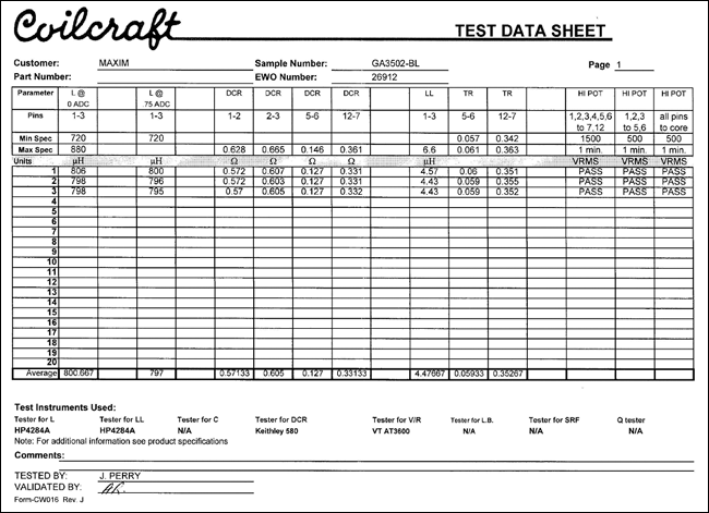
The transformer has an 18:6:1 turns ratio. Primary inductance is 800µH with a current rating of 750mA (peak) and a duty cycle always less than 50%.
The frequency of operation is 265kHz and is nonadjustable. Overvoltage protection (nonlatching) is at 120V. The UV detect level is 310V. The turn-on delay time is about 43msec, after which VIN will be about 22V and the IC will begin to drive the external MOSFET. This will, in turn, cause the VIN capacitor to decay until the bootstrap winding can provide support. Because of the high impedance of the LEDs at low voltage, the main secondary load will initially be only the output capacitor. The secondary-to-tertiary turns ratio is 6:1, which means that the bootstrap winding will supply 10V to the IC as soon as 60V develops across the output capacitor. For the 6-LED string option (i.e., with J1 installed), the output capacitor must, obviously, charge to 10.7V before 10V is available to the IC.
The calculated peak current in the primary winding of the inductor is 750mA. Leakage inductance is minimized by a split primary that sandwiches the secondary winding. The primary leakage inductance is measured at less than 5µH. Because of this low value, there is no special provision for dissipating the leakage inductance energy; all leakage energy is dissipated in the MOSFET itself. The transformer temperature rise is less than 30°C.
The switching MOSFET has an isolated tab, which allows the heatsink to be connected to ground. This minimizes the metallic surface area that experiences high-speed voltage transients, and, in turn, minimizes radiated EMI. The MOSFET sees less than a 40°C rise in temperature.
| VIN: | 400VDC ±10% |
| PWM: | N/A |
| VLED config.: |
27 LEDs (2.8VDC to 4VDC) in series (75.6VDC min to 108VDC max); 400mA With jumper: 6 LEDs (2VDC to 3VDC) in series (12V min to 18V max); 400mA |
More detailed image (PDF, 35.6kB)
Figure 1. The LED driver reference design is 1.9in x 3.9in, double sided.

More detailed image (PDF, 7.93kB)
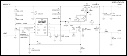
Figure 2. Schematic of the LED driver reference design.
More detailed image (PDF, 36.88kB)
Figure 3. Board layout of the LED driver.

More detailed image (PDF, 88.75kB)
Figure 4. Transformer specifications.

More detailed image (PDF, 76.43kB)
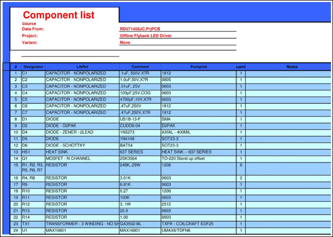
Figure 5. BOM for the reference design.
- 相关推荐
- 热点推荐
- driver
-
国家半导体:离线式TRIAC调光LED驱动器参考设计.pdf2021-08-04 1273
-
低成本离线LED驱动器2021-07-27 1529
-
离线式LED应用对LED驱动器产生的影响概述2019-09-25 1264
-
离线式电源驱动LED的应用2019-09-20 1434
-
Cirrus CS1631 9W离线LED驱动器参考设计2019-02-19 983
-
HV98101 230VAC离线式LED驱动器评估板用户指南2018-05-25 1059
-
离线高功率因数LED驱动器2011-10-08 1339
-
LED街灯应用的驱动器设计2011-09-02 1919
-
离线式LED灯对LED驱动器IC要求2011-07-14 2225
-
离线LED驱动器参考设计2010-08-04 686
-
离线型LED驱动器GreenPoint方案设计2010-03-24 827
-
符合“能源之星”标准的离线型LED驱动器参考设计2009-12-29 790
-
离线式LED驱动器参考设计2009-09-18 759
-
什么是led驱动器2009-01-19 3826
全部0条评论

快来发表一下你的评论吧 !

