
Battery Backup with Delay(具有时滞
充电电路
描述
Battery Backup with Delay(具有时滞的备用电池)
Abstract: This application note explains that the simplest link from a main supply and backup battery to a load is the diode-OR connection. However simple that concept, a diode-OR does not work when the battery voltage exceeds the main supply voltage. The article presents a circuit which handles that condition. The MAX931 comparator with 2% reference is featured in the design.
This design idea appeared in the May 25, 2006 issue of Electronic Design magazine.
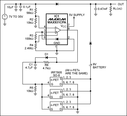
The simplest link from a main supply and backup battery to a load is the diode-OR connection. However, a diode-OR does not work when the battery voltage exceeds the main supply voltage. The Figure 1 circuit handles that condition. The main switch-mode supply voltage ranges from 7V to 30V, and the backup supply is a 9V battery.
Figure 1. IC1, the MAX931 comparator, monitors the main supply voltage. It also turns on the backup battery by grounding its negative terminal when the main supply drops below 7.4V.
The MAX931 is an ultra-low-power comparator with a 1.182V bandgap reference. During normal operation the comparator output is low, the three parallel-connected n-channel FETs are off, and the battery's negative terminal floats. Power flows from the main supply to the load. When the main voltage declines to 7.4V the comparator's output goes high, turning on the n-FETs and grounding the negative terminal of the battery. Power then flows from the battery to the load (Figure 2).
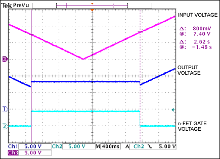
Figure 2. In response to a gradual decrease in the main supply voltage (channel 3 in Figure 1), the n-FET gate voltage goes high (channel 2). This activates the battery and drives the output voltage (channel 1) to 9V. As the main supply voltages passes 8.4V the n-FETs turn off, allowing the output to resume tracking the main supply voltage.
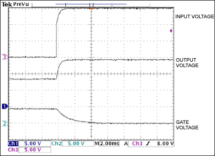
D1, C1, and R6 introduce a delay in the gate drive. This delay eliminates a supply-rail glitch that would otherwise occur when switching from the battery to the main supply. While those glitches can cause an unacceptable reset in the system's microcontroller, Figure 3 illustrates the absence of that effect with this circuit. Note that R3 and R4 set the hysteresis in the MAX931 to 800mV, as required for proper operation. See the MAX931 data sheet for calculation of those resistor values.
Figure 3. The output in Figure 1 responds without glitches in response to a fast restoration of the main supply voltage.
- 相关推荐
- 热点推荐
- B
-
具有时钟和温度的音乐频谱2023-01-05 610
-
Hat Backup System快照备份系统2022-04-28 610
-
具有时滞和的离散系统的稳定性分析2013-04-07 1165
-
具有非线性不确定性时滞系统控制算法的研究2012-02-08 752
-
TPS65510,pdf(Low-Power Battery2010-10-27 635
-
TPS3606-33,pdf(Battery-Backup2010-10-24 518
-
一类带有时变时滞的模糊双线性系统的稳定控制2009-11-09 709
-
具有实滞特性的电路图2009-07-16 694
-
Battery Selection for Secure S2009-04-20 1505
全部0条评论

快来发表一下你的评论吧 !

