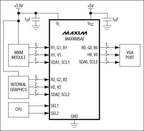

MAX4885AE应用电路图
IC应用电路图
描述
MAX4885AE应用电路图
The MAX4885AE integrates high-bandwidth analog switches, level-translating buffers, and level-translating FET switches to implement a complete 2:1 multiplexer for VGA signals. The device provides three very high-frequency 900MHz (typ) SPDT switches for RGB signals, two low-frequency clamping switches for the DDC signals, a pair of level-translating buffers for the H and V signals and integrated extended ESD protection.
Horizontal and vertical synchronization (H_/V_) inputs feature level-shifting buffers to support low-voltage controllers and standard 5V-TTL-compatible monitors, meeting the VESA requirement. Display Data Channel (DDC), consisting of SDA_ and SCL_, are FET switches that protect the low-voltage VGA source from potential damage from high-voltage presence on the monitor while reducing capacitive load.
All seven output terminals of the MAX4885AE feature high-ESD protection to ±15kV Human Body Model (HBM) (see the Pin Description in the full data sheet). All other pins are protected to ±2kV Human Body Model (HBM).
The MAX4885AE is specified over the extended -40°C to +85°C temperature range, and is available in a space-saving, 28-pin, 4mm × 4mm TQFN package.

典型工作电路
- 相关推荐
- 热点推荐
- MAX488
-
MAX4885AE高速模拟开关器相关资料分享2021-05-19 1767
-
MAX2079应用电路图2012-01-19 1845
-
MAX1113应用电路图2011-05-15 2947
-
完整2:1VGA复用器MAX4885AE(Maxim)2010-03-23 2328
-
MAX4885AE Fully integrated 2:12010-03-20 877
-
MAX4885AE中文资料,MAX4885AE是集成的宽带模2010-03-17 1640
-
MAX4885AE 宽带、VGA 2:1开关,具有±15kV2009-11-16 1676
-
MAX7应用电路图2009-07-20 821
-
MAX714应用电路图2009-05-13 1418
-
MAX16818应用电路图2009-03-31 1259
-
嘉利牌AE-10型家用电烤箱电路图2008-11-18 3971
-
max7219应用电路图2008-04-26 2604
全部0条评论

快来发表一下你的评论吧 !

