

探究关于原语的千兆以太网RGMII接口设计
电子说
描述
之前介绍MII接口时,有介绍过RGMII接口的由来,下面在贴一下:
表8‑7 MII接口介绍
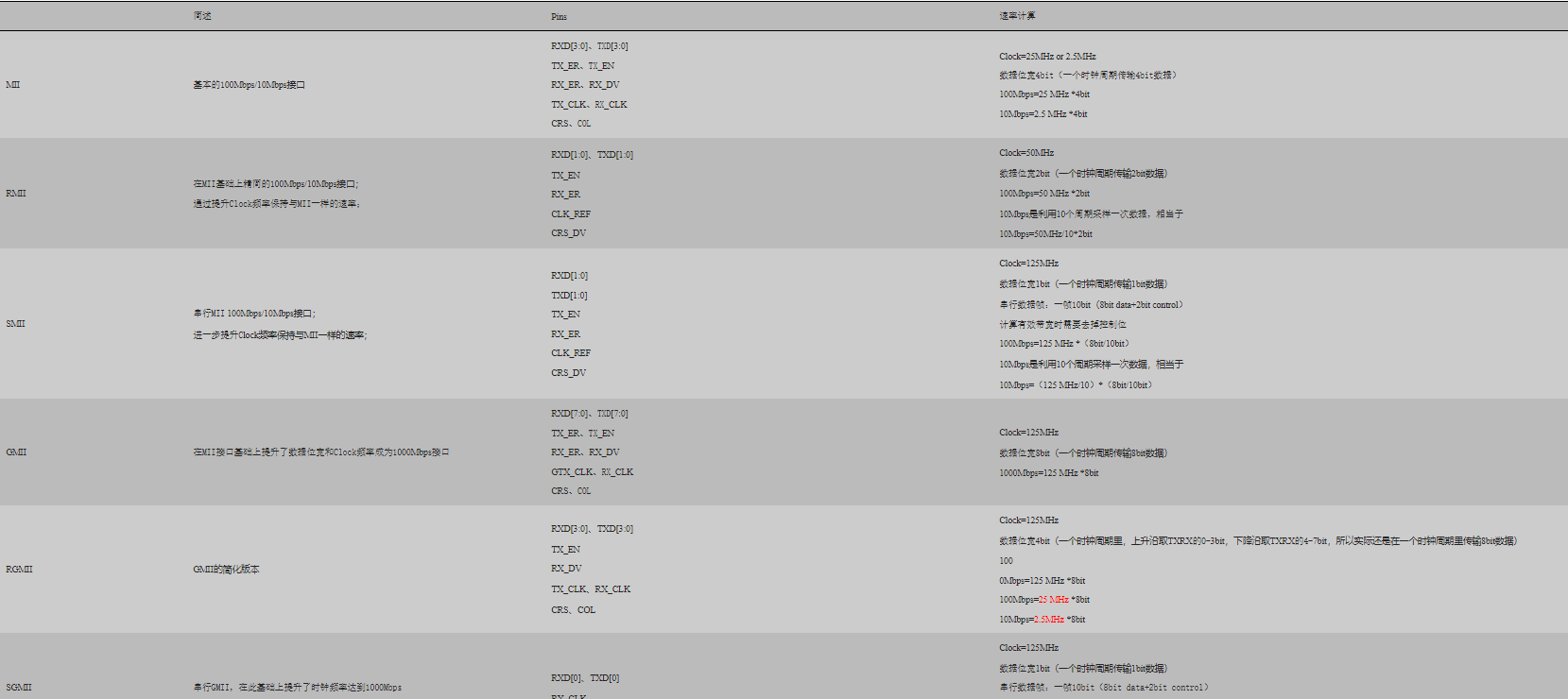
RGMII是GMII的简化版本,发送端信号:TXD[3:0]、 TX_CLK、TX_EN,接收端信号:RX_DV、RXD[3:0]、RX_CLK,当Clock=125MHz,数据位宽4bit(一个时钟周期里,上升沿取TXRX的0-3bit,下降沿取TXRX的4-7bit,所以实际还是在一个时钟周期里传输8bit数据),1000Mbps=125 MHz *8bit、100Mbps=25 MHz *8bit、10Mbps=2.5MHz *8bit。
其实从实现方式看,很容易看出RGMII传输/收取数据的方式和DDR的方式类似,所以下面会针对这方面详细介绍。8.5.1.1 RGMII信号定义及时序RGMII 使用 4bit 数据接口采用上下沿 DDR( Double Data Rate)的方式在一个时钟周期之内传输 8bit数据信号,即上升沿发送或接收数据的低 4 位[3:0],下降沿发送或接收数据的高 4 位[7:4]。
发送端:
TXC:发送数据信号和控制信号对应的同步时钟信号( 125M、 25M、 2.5M)
TXD[3:0]:发送数据信号, 4bit 位宽
TX_CTL:发送控制信号
发送端信号时序如下图所示。
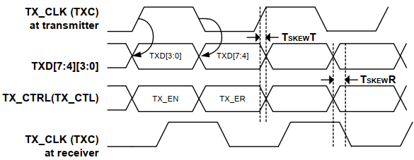
图8‑18 RGMII发送端信号时序(来源88E1512datasheet,下同)
一般的 PHY 芯片都支持两种 RGMII 发送端口的时序关系。一种称为非延时模式,如下图所示:
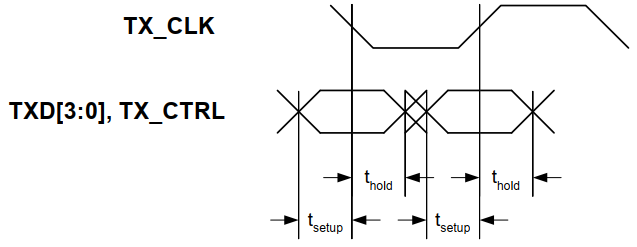
图8‑19 RGMII发送端非延时模式(来源88E1512datasheet,下同)
即要满足时钟信号 TXC 的边沿对准数据信号 TXD[3:0]和控制信号 TX_CTL 有效窗口中心附近的位置,也就是说 TXC 比其他信号存在 2ns( 90°相位)(2ns来源:当 RGMII 接口工作于 1000M 速率时, TXC 和RXC 时钟信号都为 125MHz,那么单个接口的数据率便等同于 250Mbps,单个信号的有效数据窗最大为 4ns。)左右的延时。
另一种为延时模式,如下图所示。
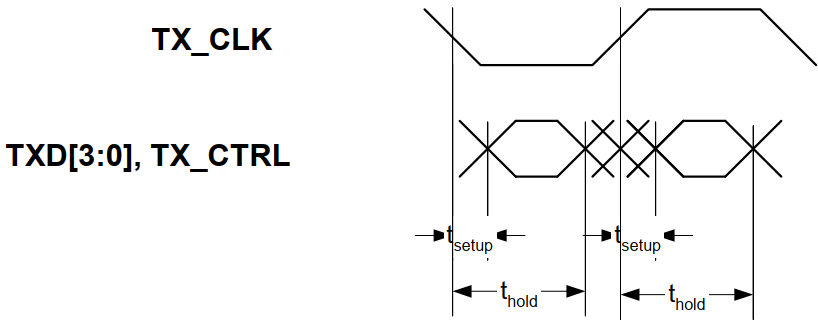
图8‑20 RGMII发送端延时模式(来源88E1512datasheet,下同)
这种时序要求 TXC 的边沿不其发送的数据 TXD 和控制信号 TX_CTL 边沿对齐,所有信号具有相同的相位。
一般来说,大部分 PHY 芯片默认都是采用正常时序模式,可通过 MDIO 接口设置寄存器,或者芯片特殊功能引脚将其配置为延时模式。
接收端:
RXC:接收数据信号和控制信号对应的同步时钟信号( 125M、 25M、 2.5M)
RXD[3:0]:接收数据信号,4bit 位宽
RX_CTL:接收控制信号
接收端信号的时序如下图所示。
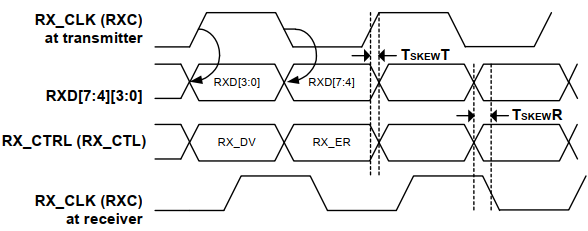
图8‑21 RGMII接收端信号时序
同理接收端也有非延时和延时模式,原理同上,时序图如下。
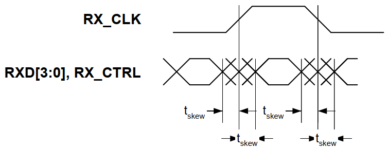
图8‑22 RGMII接收端非延时模式(来源88E1512datasheet,下同)

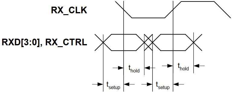
图8‑23 RGMII接收端延时模式(来源88E1512datasheet,下同)
8.5.1.2 RGMII时序中的原语使用在 FPGA 中设计高速源同步接口的重点在于时序控制和时序约束。
在 7 系列 FPGA 中实现 RGMII 接口需要借助 5 种原语,分别是:IDDR、 ODDR、 IDELAYE2、ODELAYE2(A7 中没有)、 IDELAYCTRL。
其中, IDDR 和 ODDR 分别是输入和输出的双边沿寄存器,位于 IOB 中。IDELAYE2 和ODELAYE2,分别用于控制 IO 口输入和输出延时。同时, IDELAYE2 和 ODELAYE2 的延时值需要使用原语 IDELAYCTRL 来进行校准。另外,需要注意的是,在 7 系列器件的 HR Bank 中没有ODELAYE2,只有在 HP BANK 中才有 ODELAYE2。
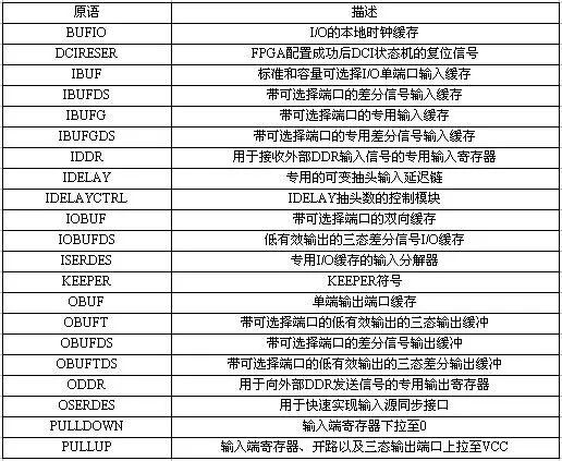
上述几个原语在Xilinx中属于I/O计算组件,其他常见的原语如下:
表8‑8 I/O端口组件
下面针对即将使用的几个原语进行介绍(摘选自米联客教程,在此谢过):
( 1) IDDR
IDDR 将输入的双边沿 DDR 信号,在输出端恢复为两个并行单边沿 SDR 信号。IDDR 的原语如下。详细参数可参考 UG471。
代码8‑1 IDDR 的原语
1.// IDDR : In order to incorporate this function into the design,
2.// Verilog : the following instance declaration needs to be placed
3.// instance : in the body of the design code. The instance name
4.// declaration : (IDDR_inst) and/or the port declarations within the
5.// code : parenthesis may be changed to properly reference and
6.// : connect this function to the design. Delete or comment
7.// : out inputs/outs that are not necessary.
8.
9.// 《-----cut code=“” below=“” this=“” line----=“”》
10.
11. // IDDR: Input Double Data Rate Input Register with Set, Reset
12. // and Clock Enable.
13. // Artix-7
14. // Xilinx HDL Language Template, version 2018.3
15.
16. IDDR #(
17. .DDR_CLK_EDGE(“OPPOSITE_EDGE”), // “OPPOSITE_EDGE”, “SAME_EDGE”
18. // or “SAME_EDGE_PIPELINED”
19. .INIT_Q1(1‘b0), // Initial value of Q1: 1’b0 or 1‘b1
20. .INIT_Q2(1’b0), // Initial value of Q2: 1‘b0 or 1’b1
21. .SRTYPE(“SYNC”) // Set/Reset type: “SYNC” or “ASYNC”
22. ) IDDR_inst (
23. .Q1(Q1), // 1-bit output for positive edge of clock
24. .Q2(Q2), // 1-bit output for negative edge of clock
25. .C(C), // 1-bit clock input
26. .CE(CE), // 1-bit clock enable input
27. .D(D), // 1-bit DDR data input
28. .R(R), // 1-bit reset
29. .S(S) // 1-bit set
30. );
31.
32. // End of IDDR_inst instantiation
33.
34.
C 为同步时钟, Q1 和 Q2 则是分别与 C 上升沿和下降沿同步的输出的 SDR 数据, D 为 DDR 输入。参数 DDR_CLK_EDGE 用来决定了 C、 Q1、 Q2 和 D 之间的时序关系。DDR_CLK_EDGE 有 3 种模式:OPPOSITE_EDGE、 SAME_EDGE 以及 SAME_EDGE_PIPELINED,3 种时序关系如下图所示。
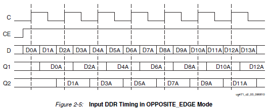
图8‑24 DDR_CLK_EDGE 3 种模式(来源UG741)
(2) ODDR
使用 ODDR 将 TXC 同一个时钟周期内的两个 SDR 信号分别通过上升沿和下降沿输出为 DDR 信号。ODDR 的原语如下,详细参数可参考 UG471。
代码8‑2 ODDR原语
1.// ODDR : In order to incorporate this function into the design,
2.// Verilog : the following instance declaration needs to be placed
3.// instance : in the body of the design code. The instance name
4.// declaration : (ODDR_inst) and/or the port declarations within the
5.// code : parenthesis may be changed to properly reference and
6.// : connect this function to the design. Delete or comment
7.// : out inputs/outs that are not necessary.
8.
9.// 《-----cut code=“” below=“” this=“” line----=“”》
10.
11. // ODDR: Output Double Data Rate Output Register with Set, Reset
12. // and Clock Enable.
13. // Artix-7
14. // Xilinx HDL Language Template, version 2018.3
15.
16. ODDR #(
17. .DDR_CLK_EDGE(“OPPOSITE_EDGE”), // “OPPOSITE_EDGE” or “SAME_EDGE”
18. .INIT(1‘b0), // Initial value of Q: 1’b0 or 1‘b1
19. .SRTYPE(“SYNC”) // Set/Reset type: “SYNC” or “ASYNC”
20. ) ODDR_inst (
21. .Q(Q), // 1-bit DDR output
22. .C(C), // 1-bit clock input
23. .CE(CE), // 1-bit clock enable input
24. .D1(D1), // 1-bit data input (positive edge)
25. .D2(D2), // 1-bit data input (negative edge)
26. .R(R), // 1-bit reset
27. .S(S) // 1-bit set
28. );
29.
30. // End of ODDR_inst instantiation
31.
32.
DDR_CLK_EDGE 有两种模式: OPPOSITE_EDGE 和 SAME_EDGE,两种时序关系如下图所示。
图8‑25 DDR_CLK_EDGE两种模式
对于 OPPOSITE_EDGE 模式,在 FPGA 内部也同样需要两个反相时钟来同步 D1 和 D2,较少使用。在设计 RGMII 接口时使用了 SAME_EDGE 模式。
(3) IDELAYE2
IDELAYE2 用于在信号通过引脚进入芯片内部之前,进行延时调节。这里给出本方案中的用法,原语描述如下。详细参数可参考 UG471。
代码8‑3 IDELAYE2 原语
1.// IDELAYE2 : In order to incorporate this function into the design,
2.// Verilog : the following instance declaration needs to be placed
3.// instance : in the body of the design code. The instance name
4.// declaration : (IDELAYE2_inst) and/or the port declarations within the
5.// code : parenthesis may be changed to properly reference and
6.// : connect this function to the design. All inputs
7.// : and outputs must be connected.
8.
9.// 《-----cut code=“” below=“” this=“” line----=“”》
10.
11. // IDELAYE2: Input Fixed or Variable Delay Element
12. // Artix-7
13. // Xilinx HDL Language Template, version 2018.3
14.
15. (* IODELAY_GROUP = *) // Specifies group name for associated IDELAYs/ODELAYs and IDELAYCTRL
16.
17. IDELAYE2 #(
18. .CINVCTRL_SEL(“FALSE”), // Enable dynamic clock inversion (FALSE, TRUE)
19. .DELAY_SRC(“IDATAIN”), // Delay input (IDATAIN, DATAIN)
20. .HIGH_PERFORMANCE_MODE(“FALSE”), // Reduced jitter (“TRUE”), Reduced power (“FALSE”)
21. .IDELAY_TYPE(“FIXED”), // FIXED, VARIABLE, VAR_LOAD, VAR_LOAD_PIPE
22. .IDELAY_VALUE(0), // Input delay tap setting (0-31)
23. .PIPE_SEL(“FALSE”), // Select pipelined mode, FALSE, TRUE
24. .REFCLK_FREQUENCY(200.0), // IDELAYCTRL clock input frequency in MHz (190.0-210.0, 290.0-310.0)。
25. .SIGNAL_PATTERN(“DATA”) // DATA, CLOCK input signal
26. )
27. IDELAYE2_inst (
28. .CNTVALUEOUT(CNTVALUEOUT), // 5-bit output: Counter value output
29. .DATAOUT(DATAOUT), // 1-bit output: Delayed data output
30. .C(C), // 1-bit input: Clock input
31. .CE(CE), // 1-bit input: Active high enable increment/decrement input
32. .CINVCTRL(CINVCTRL), // 1-bit input: Dynamic clock inversion input
33. .CNTVALUEIN(CNTVALUEIN), // 5-bit input: Counter value input
34. .DATAIN(DATAIN), // 1-bit input: Internal delay data input
35. .IDATAIN(IDATAIN), // 1-bit input: Data input from the I/O
36. .INC(INC), // 1-bit input: Increment / Decrement tap delay input
37. .LD(LD), // 1-bit input: Load IDELAY_VALUE input
38. .LDPIPEEN(LDPIPEEN), // 1-bit input: Enable PIPELINE register to load data input
39. .REGRST(REGRST) // 1-bit input: Active-high reset tap-delay input
40. );
41.
42. // End of IDELAYE2_inst instantiation
43.
44.
(4) ODELAYE2
ODELAYE2原语如下,更多详细信息可参考 UG471。
代码8‑4 ODELAYE2原语1.// ODELAYE2 : In order to incorporate this function into the design,
2.// Verilog : the following instance declaration needs to be placed
3.// instance : in the body of the design code. The instance name
4.// declaration : (ODELAYE2_inst) and/or the port declarations within the
5.// code : parenthesis may be changed to properly reference and
6.// : connect this function to the design. All inputs
7.// : and outputs must be connected.
8.
9.// 《-----cut code=“” below=“” this=“” line----=“”》
10.
11. // ODELAYE2: Output Fixed or Variable Delay Element
12. // Kintex-7
13. // Xilinx HDL Language Template, version 2018.3
14.
15. (* IODELAY_GROUP = *) // Specifies group name for associated IDELAYs/ODELAYs and IDELAYCTRL
16.
17. ODELAYE2 #(
18. .CINVCTRL_SEL(“FALSE”), // Enable dynamic clock inversion (FALSE, TRUE)
19. .DELAY_SRC(“ODATAIN”), // Delay input (ODATAIN, CLKIN)
20. .HIGH_PERFORMANCE_MODE(“FALSE”), // Reduced jitter (“TRUE”), Reduced power (“FALSE”)
21. .ODELAY_TYPE(“FIXED”), // FIXED, VARIABLE, VAR_LOAD, VAR_LOAD_PIPE
22. .ODELAY_VALUE(0), // Output delay tap setting (0-31)
23. .PIPE_SEL(“FALSE”), // Select pipelined mode, FALSE, TRUE
24. .REFCLK_FREQUENCY(200.0), // IDELAYCTRL clock input frequency in MHz (190.0-210.0, 290.0-310.0)。
25. .SIGNAL_PATTERN(“DATA”) // DATA, CLOCK input signal
26. )
27. ODELAYE2_inst (
28. .CNTVALUEOUT(CNTVALUEOUT), // 5-bit output: Counter value output
29. .DATAOUT(DATAOUT), // 1-bit output: Delayed data/clock output
30. .C(C), // 1-bit input: Clock input
31. .CE(CE), // 1-bit input: Active high enable increment/decrement input
32. .CINVCTRL(CINVCTRL), // 1-bit input: Dynamic clock inversion input
33. .CLKIN(CLKIN), // 1-bit input: Clock delay input
34. .CNTVALUEIN(CNTVALUEIN), // 5-bit input: Counter value input
35. .INC(INC), // 1-bit input: Increment / Decrement tap delay input
36. .LD(LD), // 1-bit input: Loads ODELAY_VALUE tap delay in VARIABLE mode, in VAR_LOAD or
37. // VAR_LOAD_PIPE mode, loads the value of CNTVALUEIN
38.
39. .LDPIPEEN(LDPIPEEN), // 1-bit input: Enables the pipeline register to load data
40. .ODATAIN(ODATAIN), // 1-bit input: Output delay data input
41. .REGRST(REGRST) // 1-bit input: Active-high reset tap-delay input
42. );
43.
44. // End of ODELAYE2_inst instantiation
45.
46.
(5) IDELAYCTRL
IDELAY2 和 ODELAY2 都需要 IDELAYCTRL 来进行校准。IDELAYCTRL 原语如下。更多详细信息可参考 UG471。
代码8‑5 IDELAYCTRL 原语
1.// IDELAYCTRL : In order to incorporate this function into the design,
2.// Verilog : the following instance declaration needs to be placed
3.// instance : in the body of the design code. The instance name
4.// declaration : (IDELAYCTRL_inst) and/or the port declarations within the
5.// code : parenthesis may be changed to properly reference and
6.// : connect this function to the design. All inputs
7.// : and outputs must be connected.
8.
9.// 《-----cut code=“” below=“” this=“” line----=“”》
10.
11. // IDELAYCTRL: IDELAYE2/ODELAYE2 Tap Delay Value Control
12. // Artix-7
13. // Xilinx HDL Language Template, version 2018.3
14.
15. (* IODELAY_GROUP = *) // Specifies group name for associated IDELAYs/ODELAYs and IDELAYCTRL
16.
17. IDELAYCTRL IDELAYCTRL_inst (
18. .RDY(RDY), // 1-bit output: Ready output
19. .REFCLK(REFCLK), // 1-bit input: Reference clock input
20. .RST(RST) // 1-bit input: Active high reset input
21. );
22.
23. // End of IDELAYCTRL_inst instantiation
24.
25.
IDELAYCTRL 需要一个参考时钟信号 REFCLK 来校准 IDELAY2 和 ODELAY2 每个 tap 的延时值,可用的 REFCLK 频率为 200M、 300M、 400M。时钟越高对应的 tap 延时平均值越小,也就是说延时调节精度越高。DS182 中对此有如下描述。

大部分情冴下使用 200M 的参考时钟就可以满足实际需求。
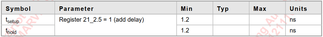
8.5.1.3 RGMII发送接口设计
(1) PHY RGMII 发送接口时序
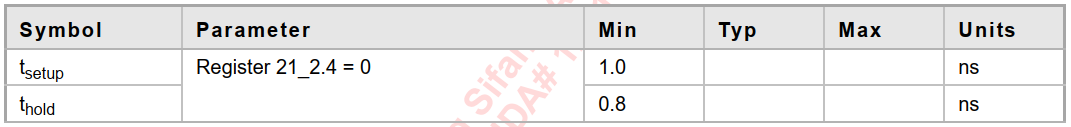
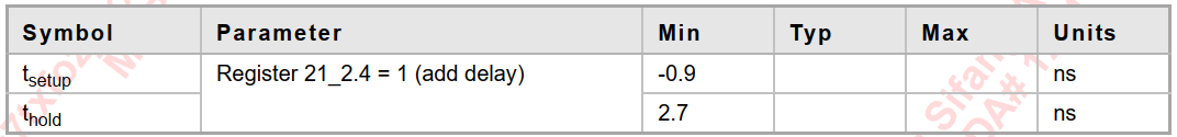
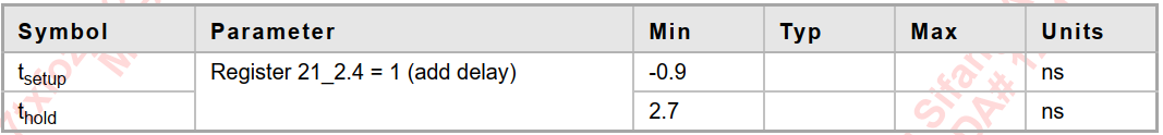
相关的时序在上面已经介绍,主要关注tsetup、thold 默认模式具体如下:
(2)设计方案
针对上述时序关系, RGMII 发送接口的设计方案如下图所示。
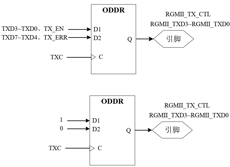
图8‑27 RGMII 发送接口的设计方案
(3)时序约束
针对 RGMII 发送接口需要进行 output delay 约束,如下所示。使用 MMCM 输出的时钟 phy_tx_clk 作为所有 ODDR 的输入时钟。这里以 1 个 RGMII 接口为例。
代码8‑6 时序约束
1.settx_clk [get_clocks -include_generated_clocks -of [get_pins clk_wiz_0/inst/mmcm_adv_inst/CLKOUT1]]
2.create_generated_clock -name phy_tx_clk -source [get_pins clk_wiz_0/inst/mmcm_adv_inst/CLKOUT1] -multiply_by1 [get_ports phy1_rgmii_tx_clk]
3.set_output_delay -clock [get_clocksphy_tx_clk] -max -0.900 [get_ports {phy1_rgmii_tx_ctl phy1_rgmii_tx_data[*]}}]
4.set_output_delay -clock [get_clocksphy_tx_clk] -min -2.900 [get_ports {phy1_rgmii_tx_ctl {phy1_rgmii_tx_data[*]}}]
5.set_output_delay -clock [get_clocksphy_tx_clk] -max -0.900 [get_ports {phy1_rgmii_tx_ctl {phy1_rgmii_tx_data[*]}}] -clock_fall -
6.add_delay
7.set_output_delay -clock [get_clocksphy_tx_clk] -min -2.900 [get_ports {phy1_rgmii_tx_ctl {phy1_rgmii_tx_data[*]}}] -clock_fall -add_delay
由于时序分析中存在 2 个时钟 phy_tx_clk 和 tx_clk,这两个时钟在物理上实际是同 1 个时钟,都是由MMCM 同 1 个引脚输出的。但是时序分析工具会把它们当做 2 个不同的时钟而进行跨时钟域分析。因此,需要剔除这 2 个时钟之间的一些虚假路径,避免时序报错。
针对本文档的设计方法,RGMII 发送接口 DDR 的 setup time 分析是从 rise 到 rise,或者 fall 到 fall。因此需要剔除 rise 到 fall 和 fall 到 rise 的 setup time 伪路径。同理, hold time 分析是从 rise 到 fall 或fall 到 rise,因此需要剔除 rise 到 rise 和 fall 到 fall 的 hold time 伪路径。如下所示:
1.set_false_path -fall_from $tx_clk -rise_to [get_clocksphy_tx_clk] -setup
2.set_false_path -rise_from $tx_clk -fall_to [get_clocksphy_tx_clk] -setup
3.set_false_path -fall_from $tx_clk -fall_to [get_clocksphy_tx_clk] -hold
4.set_false_path -rise_from $tx_clk -rise_to [get_clocksphy_tx_clk] -hold
除此之外,由于 setup time 分析是从 rise 到 rise 或fall 到 fall 的。为了避免时序分析工具对 2 个时钟phy_tx_clk 和 tx_clk 之间 setup time 进行错误的多周期分析,需要进行如下约束。
1.set_multicycle_path 0 -setup -end -rise_from $tx_clk -rise_to [get_clocksphy_tx_clk]
2.set_multicycle_path 0 -setup -end -fall_from $tx_clk -fall_to [get_clocksphy_tx_clk]
8.5.1.4 RGMII接收接口设计
(1) PHY RGMII 接收接口时序
相关的时序在上面已经介绍,主要关注tsetup、thold 默认模式具体如下:
(2)设计方案
针对上述时序关系, RGMII 接收接口的设计方案如下图所示。通过 FPGA 引脚输入的时钟 RXC 经过BUFIO 可以通过最短的延时接入 IDDR 中。另外,输入时钟经过 BUFG 或者 BUFR 进入 FPGA 内部时钟网络供内部逻辑所使用。BUFR 仅局限于单个 clock region 内部的逻辑资源,如果逻辑规模较大,建议使用 BUFG。
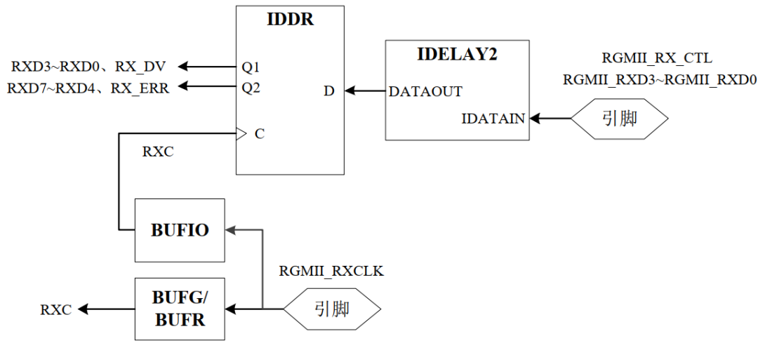
图8‑30 RGMII 接收接口的设计方案
(3)时序约束
针对 RGMII 接收接口需要进行 intput delay 约束,如下所示。使用 PHY 芯片输入时钟作为所有 IDDR的输入时钟。这里以 1 个 RGMII 接口为例。
1.create_clock -period 6.000 -name phy1_rx_clk [get_ports phy1_rgmii_rx_clk]
2.set_input_delay -clock [get_clocks phy1_rx_clk] -max 2.800 [get_ports {{phy1_rgmii_rx_data[*]} phy1_rgmii_rx_ctl}]
3.set_input_delay -clock [get_clocks phy1_rx_clk] -min 1.200 [get_ports {{phy1_rgmii_rx_data[*]} phy1_rgmii_rx_ctl}]
4.set_input_delay -clock [get_clocks phy1_rx_clk] -clock_fall -max -add_delay 2.800 [get_ports {{phy1_rgmii_rx_data[*]} phy1_rgmii_rx_ctl}]
5.set_input_delay -clock [get_clocks phy1_rx_clk] -clock_fall -min -add_delay 1.200 [get_ports {{phy1_rgmii_rx_data[*]} phy1_rgmii_rx_ctl}]
除此之外,还需要将所有 IDELAYE2 和 IDELAYCTRL 约束到一个 group 中。在 7 系列器件中, 1 个BANK 对应一个 clock region,每个 clock region 对应 1 个 IDELAYCTRL。FPGA中有 4 组 RGMII 接收接口,分布在 BANK13 和 BANK14 中。因此,需要分 2 个 group 进行约束,约束如下。
1.set_property IODELAY_GROUP iodelay_grp_bank13 [get_cells {idelayctrl_inst1 rgmii_receive_module1/delay_rgmii_rx_ctl
2.{rgmii_receive_module1/RGMII_RX_DATA_BUS[*].delay_rgmii_rxd}}]
3.set_property IODELAY_GROUP iodelay_grp_bank13 [get_cells {rgmii_receive_module2/delay_rgmii_rx_ctl
4.{rgmii_receive_module2/RGMII_RX_DATA_BUS[*].delay_rgmii_rxd}}]
5.set_property IODELAY_GROUP iodelay_grp_bank14 [get_cells {idelayctrl_inst2 rgmii_receive_module3/delay_rgmii_rx_ctl
6.{rgmii_receive_module3/RGMII_RX_DATA_BUS[*].delay_rgmii_rxd}}]
7.set_property IODELAY_GROUP iodelay_grp_bank14 [get_cells {rgmii_receive_module4/delay_rgmii_rx_ctl
8.{rgmii_receive_module4/RGMII_RX_DATA_BUS[*].delay_rgmii_rxd}}]
另外,约束每组 RGMII 接收接口的 IDELAYE2 的延时 tap 数,经尝试最佳 tap 为 14。如下所示。
1.set_property IDELAY_VALUE 14 [get_cells rgmii_receive_module1/delay_rgmii_rx_ctl] 2.set_property IDELAY_VALUE 14 [get_cells {rgmii_receive_module1/RGMII_RX_DATA_BUS[*].delay_rgmii_rxd}]
编辑:jq
-
瑞芯微(EASY EAI)RV1126B 千兆以太网电路2026-05-20 4882
-
实现具有电压转换功能的工业和汽车以太网RGMII接口2024-09-03 402
-
如何使用Vitis自带的LWIP模板进行PS端千兆以太网TCP通信?2024-04-28 8952
-
浅析以太网接口及串口转以太网技术2023-09-26 9284
-
基于FPGA的UDP RGMII千兆以太网通信方案2023-09-04 3722
-
简谈基于FPGA的千兆以太网设计2023-06-01 1356
-
CH32V307VCT6使用RGMII接口实现千兆以太网是否不具备MDC和MDIO来控制和配置PHY?2022-05-31 3628
-
如何快速分辨以太网与千兆以太网2022-05-06 6661
-
关于FPGA千兆以太网的开发2022-02-08 2680
-
基于原语的千兆以太网RGMII接口设计 精选资料推荐2021-07-20 1410
-
千兆以太网发展现状 千兆以太网技术优势2021-03-21 8987
-
基于FPGA千兆以太网的开发:以太网接口中的名词解释2021-01-18 4494
-
简谈基于FPGA的千兆以太网2018-02-03 7105
-
基于FPGA的十端口千兆以太网接口的设计与实现2009-08-29 750
全部0条评论

快来发表一下你的评论吧 !
