
基于A4982设计的DMOS微型步进马达驱动技术
控制/MCU
描述
基于A4982设计的DMOS微型步进马达驱动技术
Allegro公司的A4982是集成了电平转换和过流保护的微型步进马达驱动器,适用于双极步进马达驱动,工作在全步进,半步进,1/4步进和1/6步进模式,输出驱动能力高达35V和±2 A. A4982包括固定的离线电流调节器,兼容3.3V和5V逻辑,睡眠模式电流小于10 μA.本文介绍了A4982主要特性和优势, 功能方框图, 典型应用框图以及LP和ET封装的应用电路和PCB布局框图.
DMOS Microstepping Driver with Translator and Overcurrent Protection
The A4982 is a complete microstepping motor driver with built-in translator for easy operation. It is designed to operate bipolar stepper motors in full-, half-, quarter-, and sixteenth-step modes, with an output drive capacity of up to 35 V and ±2 A.
The A4982 includes a fixed off-time current regulator which has the ability to operate in Slow or Mixed decay modes. The ET package meets customer requirements for no smoke no fire (NSNF) designs by adding no-connect pins between critical output, sense, and supply pins. So, in the case of a pin-to-adjacent-pin short, the device does not cause smoke or fire. Additionally, the device does not cause smoke or fire when any pin is shorted to ground or left open.
The translator is the key to the easy implementation of the A4982. Simply inputting one pulse on the STEP input drives the motor one microstep. There are no phase sequence tables, high frequency control lines, or complex interfaces to program.
The A4982 interface is an ideal fit for applications where a complex microprocessor is unavailable or is overburdened. During stepping operation, the chopping control in the A4982 automatically selects the current decay mode, Slow or Mixed. In Mixed decay mode, the device is set initially to a fast decay for a proportion of the fixed off-time, then to a slow decay for the remainder of the off-time. Mixed decay current control results in reduced audible motor noise, increased step accuracy, and reduced power dissipation.
Internal synchronous rectification control circuitry is provided to improve power dissipation during PWM operation. Internal circuit protection includes: thermal shutdown with hysteresis, undervoltage lockout (UVLO), and crossover-current protection.
Special power-on sequencing is not required. The A4982 is supplied in two surface mount package, the ET, a 5 mm × 5 mm, 0.90 mm nominal overall package height QFN package, and the LP package, a 24-pin TSSOP. Both packages have exposed pads for enhanced thermal dissipation, and are lead (Pb) free (suffix –T), with 100% matte tin plated leadframes.
A4982主要特性和优势:
▪ Low RDS(ON) outputs
▪ Automatic current decay mode detection/selection
▪ Mixed and Slow current decay modes
▪ Synchronous rectification for low power dissipation
▪ Internal UVLO
▪ Crossover-current protection
▪ 3.3 and 5 V compatible logic supply
▪ Thin profile QFN and TSSOP packages
▪ Thermal shutdown circuitry
▪ Short-to-ground protection
▪ Shorted load protection
▪ Low current Sleep mode, < 10 μA
▪ No smoke no fire (NSNF) compliance (ET package)
图1.A4982功能方框图
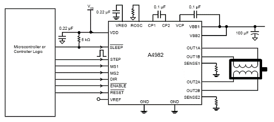
图2.A4982典型应用框图
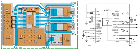
图3.A4982 LP封装应用电路和PCB布局框图
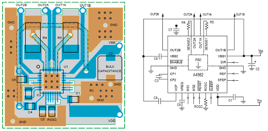
图4.A4982 ET封装应用电路和PCB布局框图
-
A4988驱动板PCB、SCH图纸2016-03-28 35672
-
步进马达驱动么控制转速的快慢2019-05-28 2381
-
广州市求购Agilent E4982A安捷伦E4982A LCR表2020-02-27 1178
-
E4982A LCR表 安捷伦E4982A 3G2020-07-22 1203
-
E4982A二手 LCR表 E4982A 3G2020-07-27 918
-
是德科技/keysightE4982A二手LCR 表2021-02-21 372
-
微型电机马达的种类有哪些?2021-06-16 2628
-
E4982A 回收新旧 E4982A2021-08-26 597
-
MS4982-双极微步进电机驱动芯片,可兼容A4982,颂扬恒科技(瑞盟一级代理)2021-12-02 818
-
双极性步进马达驱动电路2009-10-07 1116
-
HR4982_Datasheet_CN_V2.02017-08-29 1469
-
MS35774步进马达驱动在智能数控机场中的应用2024-09-03 1199
-
探索 MS35711T 步进马达驱动的奥秘2024-10-17 1184
-
HR4982内置转换器和过流保护的微特步进电机驱动芯片中文手册2025-04-14 463
-
HR4982微特步进电机驱动器:高效便捷的驱动解决方案2025-10-24 976
全部0条评论

快来发表一下你的评论吧 !

