

晶体谐振器电路应用篇
描述
关于晶体谐振器电路应用三个常见误区
关于晶体谐振器电路应用三个常见误区,晶科鑫为您整理如下:
Drive level 驱动电平
Applying excessive drive level to the crystal units may cause deterioration of characteristics or damage. Circuit design must be such as to maintain a proper drive level.
若对晶体谐振器施加过大的驱动电平,可能会导致其物理特性恶化或损坏。电路设计必须确保为晶体谐振器提供合适范围内的驱动电平。针对每一款晶体谐振器Drive level (驱动电平)的大小,晶科鑫的晶体谐振器规格书都有清晰注明。
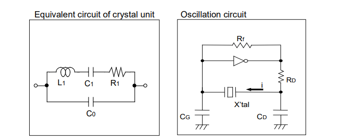
Negative resistance 负性阻抗
Unless adequate negative resistance is allocated in the oscillation circuit, oscillation start up time may increase or no oscillation may occur. In order to avoid this, provide enough negative resistance in the circuitry design.
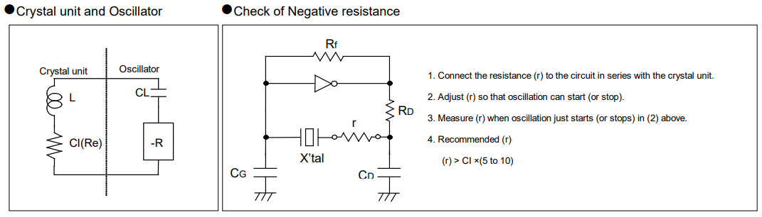
在振荡电路中如果分配的负性阻抗不够,晶体谐振器振荡的启动时间可能会延长或无振荡频率产生。请在电路设计时,提供足够负性阻抗,以确保晶体谐振器正常起振。
Load capacitance 负载电容
Differences in the load capacitance in the oscillation circuit may result in deviations in the oscillation frequency from the desired frequency. Attempting to tune by force may merely cause abnormal oscillation. Before use, please specify the load capacitance of the oscillation circuit.
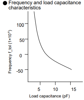
振荡电路中负载电容的差异可能导致振荡频率与期望频率产生偏差。若通过强制调谐,可能会导致晶体振荡器振荡异常。在晶体谐振器使用之前,请务必确认振荡电路的负载电容。
审核编辑:汤梓红
-
DMX-26S:表面贴装音叉型晶体谐振器与kHz带晶体谐振器2024-10-28 1228
-
DSX321G:表面贴装型晶体谐振器与MHz带晶体谐振器2024-10-14 1638
-
DSX1612S:表面贴装型晶体谐振器与MHz带晶体谐振器2024-10-08 1227
-
晶体谐振器有什么作用呢?谐振器厂家来告诉你!2023-11-08 2546
-
晶体谐振器的等效电路2022-07-04 4335
-
陶瓷谐振器与石英晶体谐振器的区别2022-04-06 4521
-
使用MEMS振荡器代替晶体谐振器的 8 大理由(一)2021-11-11 8230
-
晶体振荡器与晶体谐振器的区别2017-07-03 7957
-
石英晶体谐振器的外壳和压电特性2013-11-05 3945
-
考虑材料耗散的石英晶体谐振器电路参数的计算2008-11-24 854
-
晶体谐振器2006-04-16 1468
全部0条评论

快来发表一下你的评论吧 !
