

Linux SPI-NAND 驱动开发指南
描述
Linux SPI-NAND 驱动开发指南1 概述1.1 编写目的1.2 适用范围1.3 相关人员3 流程设计3.1 体系结构3.2 源码结构3.3 关键数据定义3.3.1 flash 设备信息数据结构3.3.2 flash chip 数据结构3.3.3 aw_spinand_chip_request3.3.4 ubi_ec_hdr3.3.5 ubi_vid_hdr3.4 关键接口说明3.4.1 MTD 层接口3.4.1.1 aw_rawnand_mtd_erase3.4.1.2 aw_rawnand_mtd_read3.4.1.3 aw_rawnand_mtd_read_oob3.4.1.4 aw_rawnand_mtd_write3.4.1.5 aw_rawnand_mtd_write_oob3.4.1.6 aw_rawnand_mtd_block_isbad3.4.1.7 aw_rawnand_mtd_block_markbad3.4.2 物理层接口3.4.2.1 aw_spinand_chip_read_single_page3.4.2.3 aw_spinand_chip_erase_single_block3.4.2.4 aw_spinand_chip_isbad_single_block3.4.2.5 aw_spinand_chip_markbad_single_block4 模块配置4.1 uboot 模块配置4.2 kernel 模块配置4.3 env.cfg
Linux SPI-NAND 驱动开发指南
1 概述
1.1 编写目的
介绍 Sunxi SPINand mtd/ubi 驱动设计, 方便相关驱动和应用开发人员
1.2 适用范围
本设计适用于所有 sunxi 平台
1.3 相关人员
Nand 模块开发人员,及应用开发人员等
2 术语、缩略语及概念
MTD:(Memory Technology device)是用于访问存储设备的 linux 子系统。本模块是MTD 子系统的 flash 驱动部分
UBI:UBI 子系统是基于 MTD 子系统的,在 MTD 上实现 nand 特性的管理逻辑,向上屏蔽nand 的特性
坏块 (Bad Block):制作工艺和 nand 本身的物理性质导致在出厂和正常使用过程中都会产生坏块
3 流程设计
3.1 体系结构
NAND MTD/UBI 驱动主要包括 5 大组件,如下图:
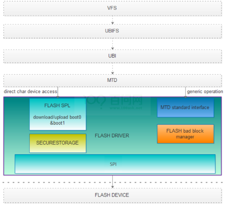
图 3-1: UBI 架构
说明:
MTD standard interface: 对接 MTD 层通用读写接口
FLASH bad block manager: 驱动层对 flash 坏块的管理
FLASH SPL: 主要是实现读写 boot0、boot1,可用于 ioctl 对boot0、boot1 的升级
SECURESTORAGE:主要是给上层提供私有数据的管理 SPI:HOST端控制器层的实现。
3.2 源码结构
kernel 源码目录:linux-5.4/drivers/mtd/awnand/spinand
.
├── Kconfig
├── Makefile
├── physic
│ ├── bbt.c
│ ├── cache.c
│ ├── core.c
│ ├── ecc.c
│ ├── id.c
│ ├── Makefile
│ ├── ops.c
│ └── physic.h
├── secure-storage.c
├── sunxi-common.c
├── sunxi-core.c
├── sunxi-debug.c
├── sunxi-nftl-core.c
└── sunxi-spinand.h
内核目录下
`-- include
`-- linux
`-- mtd
|-- aw-spinand.h
3.3 关键数据定义
3.3.1 flash 设备信息数据结构
struct aw_spinand_phy_info {
const char *Model;
unsigned char NandID[MAX_ID_LEN];
unsigned int DieCntPerChip;
unsigned int BlkCntPerDie;
unsigned int PageCntPerBlk;
unsigned int SectCntPerPage;
unsigned int OobSizePerPage;
#define BAD_BLK_FLAG_MARK 0x03
#define BAD_BLK_FLAG_FRIST_1_PAGE 0x00
#define BAD_BLK_FLAG_FIRST_2_PAGE 0x01
#define BAD_BLK_FLAG_LAST_1_PAGE 0x02
#define BAD_BLK_FLAG_LAST_2_PAGE 0x03
int BadBlockFlag;
#define SPINAND_DUAL_READ BIT(0)
#define SPINAND_QUAD_READ BIT(1)
#define SPINAND_QUAD_PROGRAM BIT(2)
#define SPINAND_QUAD_NO_NEED_ENABLE BIT(3)
#define SPINAND_ONEDUMMY_AFTER_RANDOMREAD BIT(8)
int OperationOpt;
int MaxEraseTimes;
#define HAS_EXT_ECC_SE01 BIT(0)
#define HAS_EXT_ECC_STATUS BIT(1)
enum ecc_status_shift ecc_status_shift;
int EccFlag;
enum ecc_limit_err EccType;
enum ecc_oob_protected EccProtectedType;
};
说明:
• Model:flash 的 model 名字
• NandID:flash 的 id 码
• DieCntPerChip:每 chip 的 die 个数
• BlkCntPerDie:每 die 有多少个 block
• PageCntPerBlk:每 block 有多少个 page
• SectCntPerPage:每 page 有多少个扇区
• OobSizePerPage:每 page 的 obb 大小
• BadBlockFlag:坏块标志存放在每个 block 的那个 page 中
BAD_BLK_FLAG_FRIST_1_PAGE
BAD_BLK_FLAG_FIRST_2_PAGE
BAD_BLK_FLAG_LAST_1_PAGE
BAD_BLK_FLAG_LAST_2_PAGE
• OperationOpt:支持的操作
SPINAND_DUAL_READ
SPINAND_QUAD_READ
SPINAND_QUAD_PROGRAM
SPINAND_QUAD_NO_NEED_ENABLE
SPINAND_ONEDUMMY_AFTER_RANDOMREAD
• MaxEraseTimes:最大擦除数据
• EccFlag:特性物料读 ecc status 说需目录不同
• GD5F1GQ4UCYIG 通过 0Fh + C0h 获取 ecc status,则无需配置 EccFlag
• MX35LF1GE4AB 通过 7Ch + one dummy byte 获取 ecc status,则配置 EccFlag = HAS_EXT_ECC_STATUS
• EccType:设置 ecc 值对应的状态关系
• EccProtectedType:在 spare 去选择收 ecc 保护的 16byte 作为 oob 区
例(MX35LF2GE4AD):
{
.Model = "MX35LF2GE4AD",
.NandID = {0xc2, 0x26, 0x03, 0xff, 0xff, 0xff, 0xff, 0xff},
.DieCntPerChip = 1,
.SectCntPerPage = 4,
.PageCntPerBlk = 64,
.BlkCntPerDie = 2048,
.OobSizePerPage = 64,
.OperationOpt = SPINAND_QUAD_READ | SPINAND_QUAD_PROGRAM | SPINAND_DUAL_READ,
.MaxEraseTimes = 65000,
.EccFlag = HAS_EXT_ECC_STATUS,
.EccType = BIT4_LIMIT5_TO_8_ERR9_TO_15,
.EccProtectedType = SIZE16_OFF4_LEN4_OFF8,
.BadBlockFlag = BAD_BLK_FLAG_FIRST_2_PAGE,
},
3.3.2 flash chip 数据结构
struct aw_spinand_chip {
struct aw_spinand_chip_ops *ops;
struct aw_spinand_ecc *ecc;
struct aw_spinand_cache *cache;
struct aw_spinand_info *info;
struct aw_spinand_bbt *bbt;
struct spi_device *spi;
unsigned int rx_bit;
unsigned int tx_bit;
unsigned int freq;
void *priv;
};
此结构定义了 flash chip 层的物理模型数据结构以及 chip 层对 flash 的操作接口。
• aw_spinand_chip_ops:flash 读、写、擦等操作接口
• aw_spinand_ecc:flash ecc 读、写和校验操作接口
• aw_spinand_cache:对缓存 page 的管理,提高读写效率
• aw_spinand_info:flash ID、page size 等信息及获取信息的操作接口
• aw_spinand_bbt:flash 坏块表及管理等操作接口
• spi_device:spi 父设备的操作结构体
• rx_bit:读状态操作标志
• tx_bit:写状态操作标志
3.3.3 aw_spinand_chip_request
struct aw_spinand_chip_request {
unsigned int block;
unsigned int page;
unsigned int pageoff;
unsigned int ooblen;
unsigned int datalen;
void *databuf;
void *oobbuf;
unsigned int oobleft;
unsigned int dataleft;
};
操作目标结构体,改结构体填充我们待操作的 block 的那个 page 的多少偏移的数据
databuf/oobbuf
• block:待操作块
• page:待操作页
• pageoff:操作偏移
• ooblen:操作 oob 长度
• datalen:操作数据长度
• databuf:操作目标数据
• oobbuf:操作目标 oob
3.3.4 ubi_ec_hdr
struct ubi_ec_hdr {
__be32 magic;
__u8 version;
__u8 padding1[3];
__be64 ec; /* Warning: the current limit is 31-bit anyway! */
__be32 vid_hdr_offset;
__be32 data_offset;
__be32 image_seq;
__u8 padding2[32];
__be32 hdr_crc;
} __packed;
@magic: erase counter header magic number (%UBI_EC_HDR_MAGIC)
@version: version of UBI implementation which is supposed to accept this UBI image
@padding1: reserved for future, zeroes
@ec: the erase counter
@vid_hdr_offset: where the VID header starts
@data_offset: where the user data start
@image_seq: image sequence number
@padding2: reserved for future, zeroes
@hdr_crc: erase counter header CRC checksum
EC: Erase Count,记录块的擦除次数,在 ubiattach 的时候指定一个 mtd,如果 PEB 上没有
EC,则用平均的 EC 值,写入 EC 值只有在擦除的时候才会增加 1
3.3.5 ubi_vid_hdr
struct ubi_vid_hdr {
__be32 magic;
__u8 version;
__u8 vol_type;
__u8 copy_flag;
__u8 compat;
__be32 vol_id;
__be32 lnum;
__u8 padding1[4];
__be32 data_size;
__be32 used_ebs;
__be32 data_pad;
__be32 data_crc;
__u8 padding2[4];
__be64 sqnum;
__u8 padding3[12];
__be32 hdr_crc;
} __packed;
@magic: volume identifier header magic number (%UBI_VID_HDR_MAGIC)
@version: UBI implementation version which is supposed to accept this UBI image(%UBI_VERSION)
@vol_type: volume type (%UBI_VID_DYNAMIC or %UBI_VID_STATIC)
@copy_flag: if this logical eraseblock was copied from another physical eraseblock(for wear-leveling reasons)
@compat: compatibility of this volume(%0, %UBI_COMPAT_DELETE, %UBI_COMPAT_IGNORE,%UBI_COMPAT_PRESERVE, or %UBI_COMPAT_REJECT)
@vol_id: ID of this volume
@lnum: logical eraseblock number
@padding1: reserved for future, zeroes
@data_size: how many bytes of data this logical eraseblock contains
@used_ebs: total number of used logical eraseblocks in this volume
@data_pad: how many bytes at the end of this physical eraseblock are not used
@data_crc: CRC checksum of the data stored in this logical eraseblock
@padding2: reserved for future, zeroes
@sqnum: sequence number
@padding3: reserved for future, zeroes
@hdr_crc: volume identifier header CRC checksum
参数说明
@sqnum 是创建此 VID 头时的全局序列计数器的值。每次 UBI 写一个新的 VID 头到 flash 时,全局序列计数器都会增加,比如当它将一个逻辑的 eraseblock 映射到一个新的物理的 erase-block 时。全局序列计数器是一个无符号 64 位整数,我们假设它永远不会溢出。@sqnum(序列号) 用于区分新旧版本的逻辑擦除块。
有两种情况,可能有多个物理 eraseblock 对应同一个逻辑 eraseblock,即在卷标识头中有相同的 @vol_id 和 @lnum 值。假设我们有一个逻辑的擦除块 L,它被映射到物理的擦除块 P。
因为 UBI 可以异步擦除物理上的擦除块,所以可能出现以下情况:L 被异步擦除,所以 P 被安排擦除,然后 L 被写入,即。映射到另一个物理的擦除块 P1,所以 P1 被写入,然后不干净的重启发生。结果-有两个物理的 eraseblock P 和 P1 对应同一个逻辑的 eraseblock L。但是 P1 的序列号更大,所以 UBI 在连接 flash 时选择 P1。
UBI 不时地将逻辑擦除块移动到其他物理擦除块,以达到损耗均衡的目的。例如,如果 UBI将 L 从 P 移动到 P1,在 P 被物理擦除之前会发生不干净的重启,有两个物理擦除块 P 和 P1 对应于 L, UBI 必须在 flash 连接时选择其中一个。@sqnum 字段表示哪个 PEB 是原始的 (显然 P 的 @sqnum 更低) 和副本。但是选择具有更高序列号的物理擦除块是不够的,因为不干净的重新引导可能发生在复制过程的中间,因此 P 中的数据被损坏(P->P1 没复制完)。仅仅选择序号较低的物理擦除块是不够的,因为那里的数据可能很旧 (考虑在复制之后向 P1 添加更多数据的情况)。此外,不干净的重启可能发生在擦除 P 刚刚开始的时候,所以它会导致不稳定的 P,“大部分” 是 OK 的,但仍然有不稳定的情况。
UBI 使用 @copy_flag 字段表示这个逻辑擦除块是一个副本。UBI 还计算数据的 CRC,当数据被移动时,并将其存储在副本 (P1) 的 @data_crc 字段。因此,当 UBI 需要从两个 (P 或 P1)中选择一个物理擦除块时,会检查新块 (P1) 的 @copy_flag。如果它被清除,情况就简单了,新的就会被选中。如果设置了该值,则检查副本 (P1) 的数据 CRC。如果 CRC 校验和是正确的,这个物理擦除块被选中 (P1)。否则,将选择较老的 P。如果是静态卷,@data_crc 字段包含逻辑擦除块内容的 CRC 校验和。对于动态卷,它不包含 CRC 校验和规则。唯一的例外情况是,当物理擦除块的数据被磨损均衡子系统移动时,磨损均衡子系统计算数据 CRC,并将其存储在 @data_crc 字段中。
@used_ebs 字段仅用于静态卷,它表示该卷的数据需要多少个擦除块。对于动态卷,这个字段不被使用并且总是包含 0。
@data_pad 在创建卷时使用对齐参数计算。因此,@data_pad 字段有效地减少了该卷的逻辑擦除块的大小。当一个人在 UBI 卷上使用面向块的软件 (比如,cramfs) 时,这是非常方便的。
LEB 与 PEB
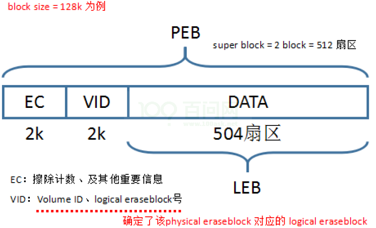
图 3-2: PEB-LEB
3.4 关键接口说明
3.4.1 MTD 层接口
3.4.1.1 aw_rawnand_mtd_erase
static int aw_rawnand_mtd_erase(struct mtd_info *mtd, struct erase_info *instr)
description:mtd erase interface
@mtd:MTD device structure
@instr:erase operation descrition structure
return:success return 0,fail return fail code
3.4.1.2 aw_rawnand_mtd_read
static int aw_rawnand_mtd_read(struct mtd_info *mtd, loff_t from, size_t len,size_t *retlen, u_char *buf)
description:mtd read interface
@mtd:MTD device structure
@from:offset to read from MTD device
@len: data len
@retlen:had read data len
@buf:data buffer
return:success return max_bitflips,fail return fail code
3.4.1.3 aw_rawnand_mtd_read_oob
static int aw_rawnand_mtd_read_oob(struct mtd_info *mtd, loff_t from, struct mtd_oob_ops *ops)
description:mtd read data with oob
@mtd:MTD device structure
@ops:oob eperation descrition structure
return:success return max_bitflips,fail return fail code
3.4.1.4 aw_rawnand_mtd_write
static int aw_rawnand_mtd_write(struct mtd_info *mtd, loff_t to, size_t len, size_t *retlen, const u_char *buf)
description:mtd write data interface
@to:offset to MTD device
@len:want write data len
@retlen:return the writen len
@buf:data buffer
return:success return 0, fail return code fail
3.4.1.5 aw_rawnand_mtd_write_oob
static int aw_rawnand_mtd_write_oob(struct mtd_info *mtd, loff_t to, struct mtd_oob_ops * ops)
description:write data with oob
@mtd:MTD device structure
@to:offset to MTD device
@ops:oob operation descrition structure
return:success return 0, fail return code fail
3.4.1.6 aw_rawnand_mtd_block_isbad
static int aw_rawnand_mtd_block_isbad(struct mtd_info *mtd, loff_t ofs)
description:check block is badblock or not
@mtd:MTD device structure
@ofs: offset the mtd device start (align to simu block size)
return:true if the block is bad, or false if the block is good
3.4.1.7 aw_rawnand_mtd_block_markbad
static int aw_rawnand_mtd_block_markbad(struct mtd_info *mtd, loff_t ofs)
description:mark block at the given offset as bad block
@mtd:MTD device structure
@ofs:offset the mtd device start
return:success to mark return 0, or fail return fail code.
3.4.2 物理层接口
3.4.2.1 aw_spinand_chip_read_single_page
static int aw_spinand_chip_read_single_page(struct aw_spinand_chip *chip, struct aw_spinand_chip_request *req)
description:Read physics on a page
@chip:See 3.3.2
@req:See 3.3.3
return:zero on success, else a negative error code.
3.4.2.2 aw_spinand_chip_write_single_page
static int aw_spinand_chip_write_single_page(struct aw_spinand_chip *chip, struct aw_spinand_chip_request *req)
description:Write physics on a page
@chip:See 3.3.2
@req:See 3.3.3
return:zero on success, else a negative error code.
3.4.2.3 aw_spinand_chip_erase_single_block
static int aw_spinand_chip_erase_single_block(struct aw_spinand_chip *chip, struct aw_spinand_chip_request *req)
description:Erase physics on a block
@chip:See 3.3.2
@req: See 3.3.3
return:zero on success, else a negative error code.
3.4.2.4 aw_spinand_chip_isbad_single_block
static int aw_spinand_chip_isbad_single_block(struct aw_spinand_chip *chip, struct aw_spinand_chip_request *req)
description:Set to bad block
@chip:See 3.3.2
@req:See 3.3.3
return:zero on success, else a negative error code.
3.4.2.5 aw_spinand_chip_markbad_single_block
static int aw_spinand_chip_markbad_single_block(struct aw_spinand_chip *chip, struct aw_spinand_chip_request *req)
description:Set to bad block
@chip:See 3.3.2
@req:See 3.3.3
return:zero on success, else a negative error code.
4 模块配置
4.1 uboot 模块配置
Device Drivers-->Sunxi flash support--> [*]Support sunxi nand devices [*]Support sunxi nand ubifs devices [*]Support COMM NAND V1 interface
如下图:
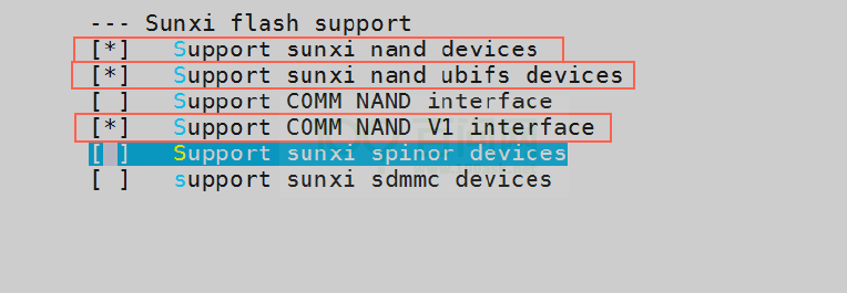
图 4-1: u-boot-spinand-menuconfig
4.2 kernel 模块配置
Device Drivers->Memory Technology Device(MTD) support-->sunxi-nand
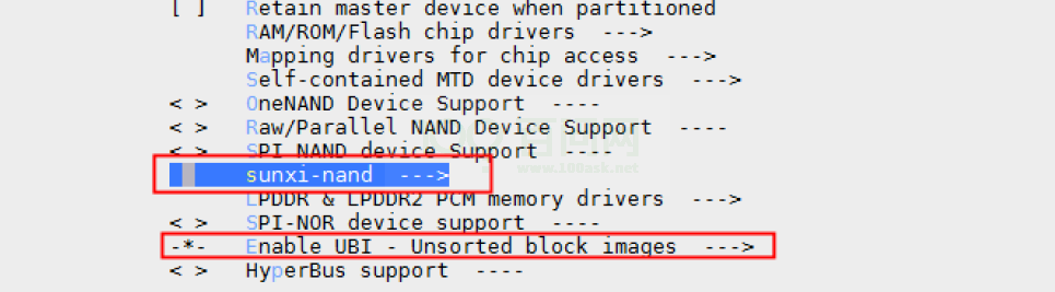
图 4-2: UBI
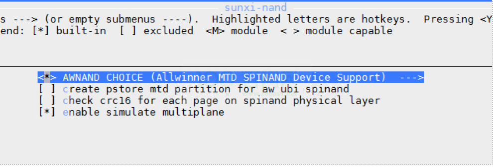
图 4-3: ker_nand-cfg
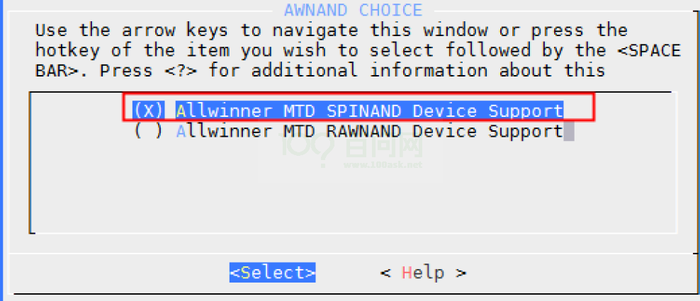
图 4-4: ker_spinand
Device Drivers->SPI support
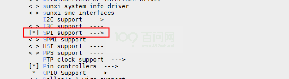
图 4-5: spi-1
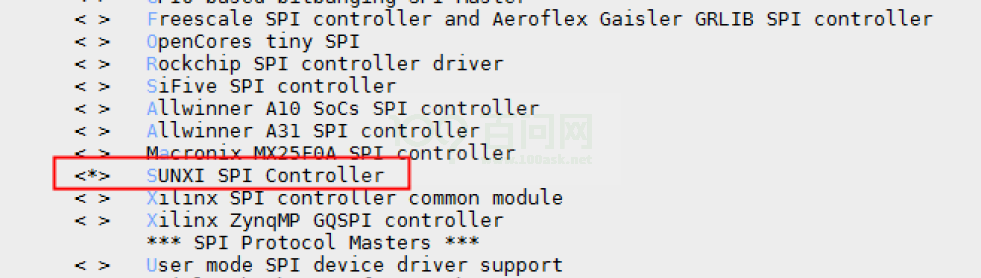
图 4-6: spi-2
Device Drivers->DMA Engine support
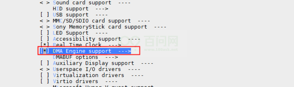
图 4-7: DMA-1
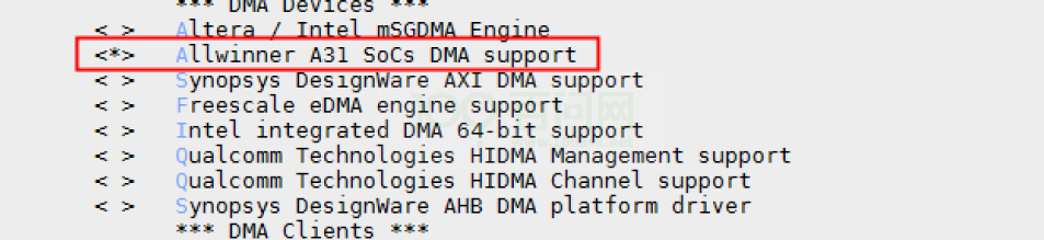
图 4-8: DMA-2
Device Drivers->SOC(System On Chip)
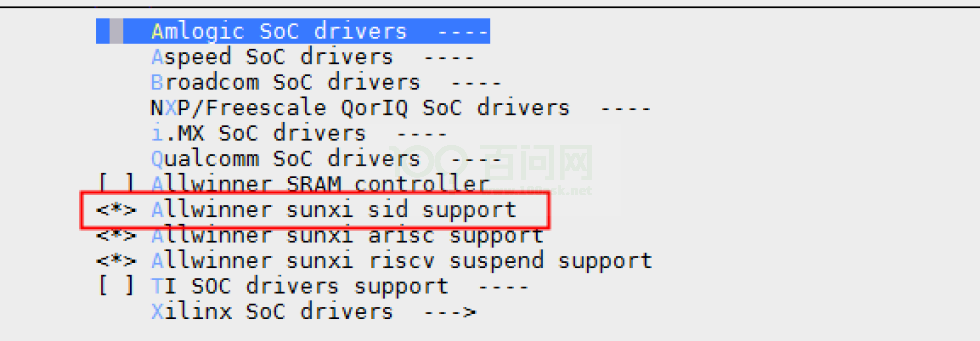
图 4-9: SID
File systems-->Miscellaneous filesystems-->
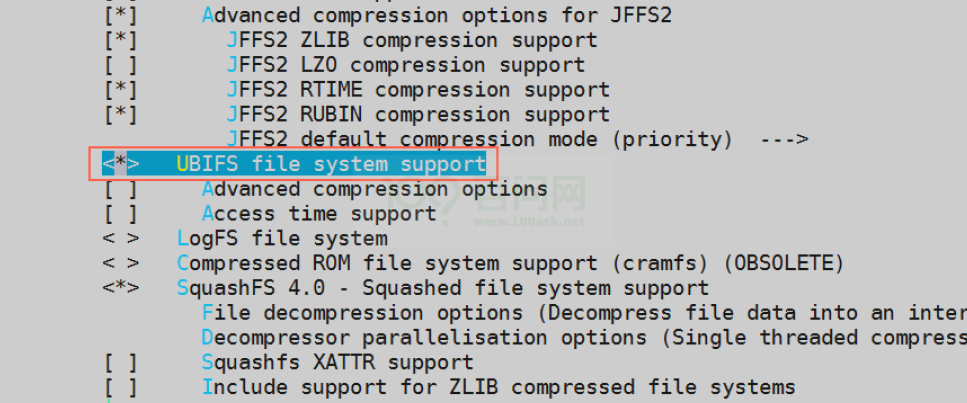
图 4-10: menuconfig_spinand_ubifs
4.3 env.cfg
在 env.cfg 中添加修改下值,setargs_nand_ubi 先 copy 一份 setargs_nand 再添加对应变量

图 4-11: build-mkcmd
审核编辑 黄宇
-
RK 平台 SPI 开发完全指南(驱动 + 配置 + 测试 + 优化)2026-01-30 1942
-
FAQ_MA35_Family_Linux 如何从没有 NAND 的 SPI-NAND 启动?2025-09-02 403
-
迅为RK3568开发板驱动指南Linux中通用SPI设备驱动2025-01-23 4443
-
没有SPI-Nand, NAND无法启动怎么解决?2023-09-06 725
-
Linux NOR开发指南2023-03-06 2698
-
Tina_Linux_系统软件开发指南2023-03-02 5784
-
Rockchip Linux SDK的开发指南的详细资料说明2020-01-10 2560
-
EAC0945 linux开发指南2017-09-28 2416
-
A64开发板LCD开发指南2016-06-21 1212
-
【图书分享】《Linux驱动开发指南——基于ARM9处理器》2014-03-18 16449
-
linux驱动开发指南基于arm9处理器2013-08-13 4143
-
Tiny6410 Linux开发指南详解2011-07-08 2132
全部0条评论

快来发表一下你的评论吧 !
