

利用DS1841对数电阻优化雪崩光电二极管(APD)的偏置范围
描述
本文阐述了如何使用DS1841对数电位器调节APD偏置电路的输出范围。为了使调节过程更简单,本文还提供了电子数据表。
APD偏置电路
DS1841可受温度控制的非易失(NV)、I²C对数电位器包含了一个7位对数变化的电阻器。通过与升压型DC-DC转换器相配合,DS1841能够调节施加在雪崩光电二极管的偏置电压。利用三个外部电阻(RSER、RTOP和RPAR)调节输出范围(图1)。
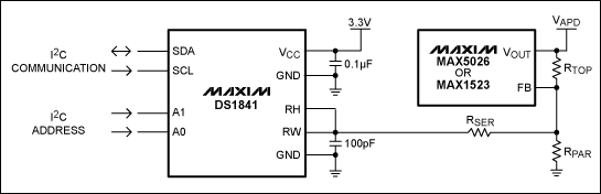
图1. 利用DS1841和升压型DC-DC转换器(此处为MAX5026或MAX1523)构成的APD偏置电路
调节APD偏置电压范围
利用电子数据表DS1841 APD偏置电压调节(xls)可以方便地调节APD偏置电压。该电子数据表包含四个输入变量:RTOP、RSER、RPAR以及VFB。输入这些电阻值后,电子数据表即可计算出四个输出值:VAPD (最大值)、VAPD (最小值)、STEP (最大值)和STEP (平均值)。此外还生成了两个曲线图:APD偏置与DAC码关系曲线和每级电压与DAC码的关系曲线图。图2所示界面给出了四个变量以及通过输入值而生成的图形。表1定义了电子数据表所使用的参数。
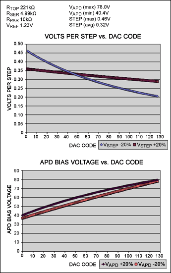
图2. 该电子数据表界面包含了四个数据输入变量(见左上角)
表1. 使用DS1841调节APD偏置电压范围时的变量定义
| VFB | The voltage present at the feedback node of the DC-DC converter. |
| VAPD (max) | The maximum voltage to which the APD bias can be set under worst-case conditions. |
| VAPD (min) | The minimum voltage to which the APD bias can be set under worst-case conditions. |
| STEP (max) | The maximum calculated voltage step that can occur between two adjacent DAC codes. |
| STEP (avg) | The average voltage step size that occurs across the full range. |
| VSTEP +20% | The voltage step size when the variable resistor is at the maximum of the process range (+20%). |
| VSTEP -20% | The voltage step size when the variable resistor is at the minimum of the process range (-20%). |
| VAPD +20% | The APD bias voltage when the variable resistor is at the maximum of the process range (+20%). |
| VAPD -20% | The APD bias voltage when the variable resistor is at the minimum of the process range (-20%). |
审核编辑:郭婷
声明:本文内容及配图由入驻作者撰写或者入驻合作网站授权转载。文章观点仅代表作者本人,不代表电子发烧友网立场。文章及其配图仅供工程师学习之用,如有内容侵权或者其他违规问题,请联系本站处理。
举报投诉
-
雪崩光电二极管(APD)的常见问题汇总与解答2026-04-14 467
-
APD雪崩光电二极管的使用方法及核心信息讲解2025-10-21 2801
-
AN92-用于雪崩光电二极管的偏置电压和电流检测电路2025-01-09 761
-
PIN光电二极管与APD雪崩二极管的优缺点介绍2024-05-22 9099
-
如何利用DS1841对数电阻优化雪崩光电二极管偏置范围2023-04-07 1957
-
雪崩光电二极管基础知识点汇总2023-02-06 3246
-
雪崩光电二极管的AN92型偏置电压和电流检测电路2021-05-07 1491
-
雪崩光电二极管的主要特性_雪崩光电二极管的工作原理2019-08-01 14588
-
DS1842 集成雪崩光电二极管(APD)偏置的分立高压元2011-04-08 2333
-
雪崩光电二极管,雪崩光电二极管是什么意思2010-02-27 1793
-
雪崩光电二极管(APD)偏置电源及其电流监测2009-07-18 6224
-
利用DS1841对数电阻优化雪崩光电二极管(APD)的偏置范2009-04-28 1169
全部0条评论

快来发表一下你的评论吧 !
