

基于MAX5941B PWM控制器的用电设备(PD)模块参考设计
描述
MAX5941B PD模块适合多种应用。图1给出了将来自交换机的数据输出连接到中跨输入的典型应用。然后,中跨将电源添加到每一个支持PoE的输出。
本例中,端口1连接到以太网相机,端口2连接到一个无线接入点。当中跨打开(或当器件连接)时,中跨检查每个输出的PoE信号。该模块将端口1及端口2的外设识别为有效的PoE设备,中跨为外设提供数据和电源。 中跨连续监测每个输出,以观察是否已添加或移除有效的PoE设备。由于本例中其他端口没有PoE信号,因此中跨仅向连接的周边设备传递数据。
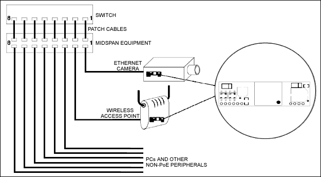
图1. 典型应用中,来自交换机的数据输出连接至中跨,通过中跨将电源添加到数据线上,实现以太网供电。
特性
兼容IEEE 802.3af
36V至60V输入电压范围
12V/1A输出
无最小负载要求
小尺寸SIL封装
低输出纹波及噪声
高效率用电设备
无需外部电容
可调输出电压
低成本
1500V隔离(输入至输出)
板上“或”逻辑二极管,带外部12V适配器
引脚说明
图2. 引脚排列
| Pin Number | Name | Description |
| 1 | VA1 | Rx Input (1) This input pin is used in conjunction with VA2 and connects to the center tap of the transformer connected to pins 1 and 2 of the RJ45 connector (Rx)—it is not polarity sensitive. |
| 2 | VA2 | Tx Input (2) This input pin is used in conjunction with VA1 and connects to the center tap of the transformer connected to pins 3 and 6 of the RJ45 connector (Tx)—it is not polarity sensitive. |
| 3 | VB1 | Direct Input (1) This input pin is used in conjunction with VB2 and connects to pins 4 and 5 of the RJ45 connector—it is not polarity sensitive. |
| 4 | VB2 | Direct Input (2) This input pin is used in conjunction with VB1 and connects to pins 7 and 8 of the RJ45 connector—it is not polarity sensitive. |
| 5 | CP1 | Class Programming (1) Connecting an external resistor to CP2 will change the current class of the module. With no resistor fitted the module will default to Class 0. |
| 6 | CP2 | Class Programming (2) Connecting an external resistor to CP1 will change the current class of the module. With no resistor fitted the module will default to Class 0. |
| 7 | GND | Ground The ground return for the output. |
| 8 | VOUT | DC Output This pin provides the regulated output voltage from the DC-DC converter. |
| 9 | ADJ | Output Adjust The output voltage can be adjusted from its nominal output by connecting an external resistor from this pin to either the VOUT pin or GND pin. |
| 10 | N.C. | No Connection This pin is not connected internally. |
功率分级
功率分级用于PD向供电设备(PSE)指示其自身功率需求的。MAX5941B模块允许通过连接在CP1的CP2之间的电阻外部编程电流分级,如图3所示。如果没有安装电阻器,模块将默认为0级。表2提供了编程电阻值的完整清单。
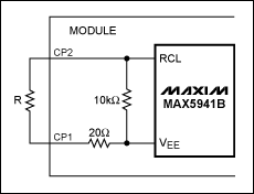
图3. 设置功率分级时,需在引脚CP1和CP2间接电阻
| Class | Programming Resistance (Ω) | Minimum Power (W) | Maximum Power (W) |
| 0 | Do not fit | 0.44 | 12.95 |
| 1 | 770 | .44 | 3.84 |
| 2 | 388 | 3.84 | 6.49 |
| 2 | 388 | 3.84 | 6.49 |
| 3 | 242 | 6.49 | 12.95 |
| 4 | 161 | Reserved | Reserved |
可调节输出
MAX5941B PD模块的ADJ引脚可将输出电压在标称值附近上下微调。调节输出电压时,在ADJ引脚与GND或VOUT之间连接电阻(图4)。用公式1和2可计算出实现预期的上调电压及下调输出电压所需的电阻值。
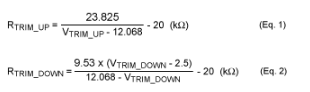
其中VTRIM_UP为预期的上调输出电压,VTRIM_DOWN为预期的下调输出电压。
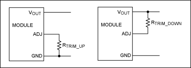
图4. 调节输出电压时,ADJ引脚与GND之间(上调)或VOUT之间(下调)连接电阻。
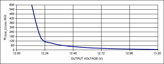
图5A. 上调输出电压曲线
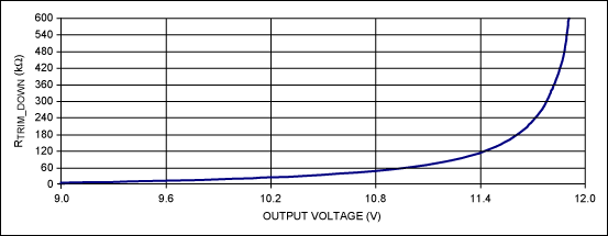
图5. 下调输出电压曲线
与外部12V适配器的典型连接
通常情况下,PD与适配器配合使用,每个输出端串接一个二极管,如图6所示。
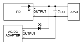
图6. 传统方案中,用电设备连接到适配器,每个输出端串接一个二极管。
对于MAX5941B PD模块,内置了输出二极管D1。如果PD单独使用,用一个0Ω电阻取代该二极管,以提高效率。图7为板上“或”逻辑二极管D1的位置。
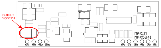
图7. 在MAX5941B PD模块中内部二极管D1的位置
该模块只需要一个外部电容,如图8所示;至少需要1µF陶瓷电容。
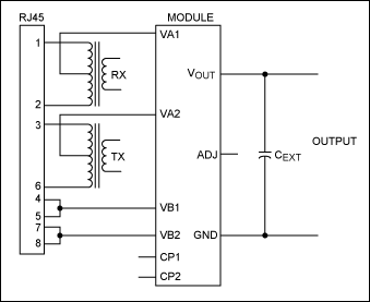
图8. 典型连接电路图中,外部电容连接在GND和VOUT之间
电气特性
| Parameter | Min | Typ | Max | Units |
| DC Supply Voltage | -.3 | 60 | V | |
| DC Supply Voltage Surge for 1ms | -.6 | 80 | V | |
| Storage Temperature | -40 | +100 | °C |
工作在超过“极限参数”中所列出的条件下将可能引起模块的永久损坏。这里只指的是极限参数,并不是意味着在这些条件下或超过这些条件下模块能正常工作。器件工作在极限参数条件下过长时间将影响模块的可靠性。
| Parameter | Min | Typ | Max | Units |
| Input Supply Voltage | 36 | 48 | 60 | V |
| Undervoltage Lockout | 30 | 36 | V | |
| Operating Temperature | -40 | 25 | +85 | C° |
| Parameter | Min | Typ | Max | Units |
| Nominal Output Voltage (Without the ORing Diode) | 11.76 | 12 | 12.24 | V |
| Output Current | 0 | 1 | A | |
| Output Ripple and Noise | 250 | mV | ||
| Efficiency Without the ORing Diode (48V Input, 1A Output) | 85 | % | ||
| Efficiency with the ORing Diode (48V Input, 1A Output) | 82 | % | ||
| Isolation Voltage | 1500 | V |
波形
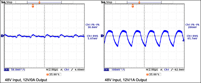
图9. 输出纹波和噪声
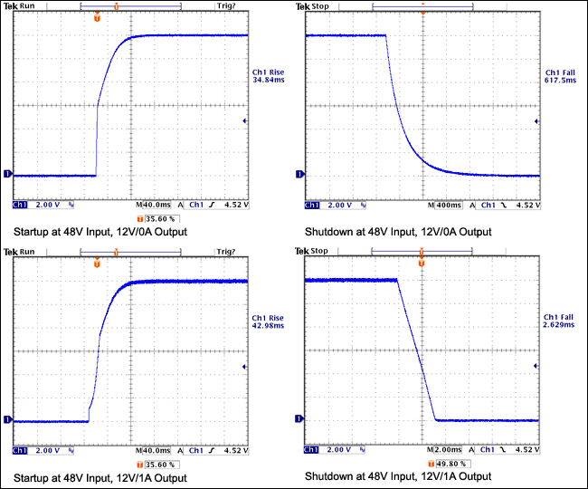
图10. 开启与关断
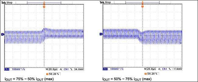
图11. 瞬态响应
器件列表
| Designation | Qty | Description |
| C1, C2, C6, C17 | 4 |
10µF 25V ceramic capacitor 1206 TDK C3216X5R1E106K MURATA GRM31CR61E106KA12 |
| C3 | 1 |
6800pF 100V ceramic capacitor 0603 TDK C1608X7R2A682K |
| C4 | 1 | 100pF 50V ceramic capacitor 0603 |
| C4 | 1 | 100pF 50V ceramic capacitor 0603 |
| C5, C7, C23 | 1 | 0.1µF 50V ceramic capacitor 0603 |
| C9 | 1 |
10µF 100V aluminium electrolytic capacitor SANYO 100CE10FS |
| C9 | 1 |
10µF 100V aluminium electrolytic capacitor SANYO 100CE10FS |
| C10 | 1 |
1000pF 1.5kV ceramic capacitor 1808 TDK C4520X7R3D102K |
| C12, C25 | 2 |
0.1µF 100V ceramic capacitor 1206 TDK C3216X7R2A104K |
| C13 | 1 |
220µF 25V aluminium electrolytic capacitor SANYO 25CE220FSA |
| C14 | 1 |
1000pF 100V ceramic capacitor 0805 TDK C2012X7R2A102K |
| C19 | 1 |
2.2µF 10V ceramic capacitor 0603 MURATA GRM188R61A225KE34 |
| C22 | 1 | 680pF 50V ceramic capacitor 0603 |
| C28 | 1 | 4700pF 50V ceramic capacitor 0603 |
| D1, D2 | 1 | Bridge rectifier DIODES HD01-T |
| D4, D6 | 2 | Diode 200mA 250V SOD323 DIODES BAV21WS |
| D5, D13 | 2 | 60V Schottky rectifier SMA DIODES B360A |
| D7 | 1 | SMT LED Lamp 0603 FAIRCHILD QTLP600C-Y |
| D8 | 1 | Transient Voltage Suppressor DIODES SMAJ54A |
| R1 | 1 | 20Ω ±1% resistor 0603 |
| R5 | 1 | 270mΩ ±1% resistor 1206 |
| R9 | 1 | 470Ω ±1% resistor 0603 |
| R10 | 1 | 10Ω ±1% resistor 1206 |
| R11, R17 | 2 | 10kΩ ±1% resistor 0603 |
| R12 | 1 | 20kΩ ±1% resistor 0603 |
| R14 | 1 | 25.5kΩ ±1% resistor 1206 |
| R15 | 1 | Not Used |
| R16 | 1 | 0Ω ±1% resistor 1206 |
| R18 | 1 | 1kΩ ±1% resistor 0805 |
| R22 | 1 | 9.53kΩ ±1% resistor 0603 |
| R23 | 1 | 2.49kΩ ±1% resistor 0603 |
| R24, R31 | 2 | 2.5kΩ ±1% resistor 0603 |
| R25, R27 | 2 | 1kΩ ±1% resistor 0603 |
| R26 | 1 | 4.75kΩ ±1% resistor 0603 |
| R28 | 1 | 33kΩ ±1% resistor 0805 |
| R30 | 1 | 4.7Ω ±1% resistor 0805 |
| Q1 | 1 | MOSFET 150V SO-8 IR IRF7465TR |
| U2 | 1 | IC Optocoupler NEC PS2801-1-F4-R-A |
| U3 | 1 | IC VREF 2.5V 0.4% SOT-23 AAC AZ431AN-A |
| U5 | 1 | PWM controller for PD MAXIM MAX5941BESE |
| R30 | 1 | Transformer NP:NS:NB = 35:16:20 LP = 122µH GA3271-AL Coilcraft |
变压器设计
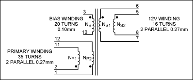
图12. 变压器电气原理图
| Parameter | Conditions | Value |
| Electrical Strength | 50Hz 1 minute, from pins 1–3, 10–12 to pins 5–8 | 1500VRMS |
| Primary Inductance | Pins 1, 12; all windings open. Measure at 275kHz |
120µH ±10% |
| Primary Leakage Inductance | Pins 1, 12; rest of pins shorted. Measure at 275kHz | 3µH (max) |
| Item | Description |
| 1 | Core: EFD15, PC40. Manufacturer: TDK |
| 2 | Bobbin: EFD15 coil former (SMD), 12 pins |
| 3 | Tape: 8.9mm wide insulation tape |
| 3 | Tape: 8.9mm wide insulation tape |
| 3 | Tape: 8.9mm wide insulation tape |
| 4 | Magnet Wire: .25mm diameter with 150°C |
| 5 | Magnet Wire: .27mm diameter with 150°C |
| 6 | Magnet wire: 0.10mm diameter with 150°C |
| 7 | Varnish |
| Note | All wires include insulation |
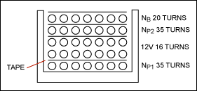
图13. 变压器构造图
| Step | Description |
| Primary NP1 | Start at pin 1. Wind 35 turns of item 4 in approximately 1 layer. Finish on Pin 12 |
| Insulation | Use 1 layer of item 3 for insulation |
| 12V Winding | Start at pins 6 and 5. Wind 16 turns of 2 parallel strands of item 5. Finish at pins 7 and 8 |
| Insulation | Use 1 Layer of Item 3 for Safety Insulation |
| Primary NP2 | Start at pin 2. Wind 35 turns of item 4 in approximately 1 layer. Finish on pin 11 |
| Insulation | Use one layer of item 3 for safety insulation |
| Bias Winding | Start at pin 3. Wind 20 turns of item 6. Spread turns evenly across bobbin. Finish at pin 10 |
| Outer Wrap | Wrap Wwndings with 2 layers of item 3 |
| Final Assembly | Assemble and secure core halves. Varnish impregnate with item 9 |
审核编辑:郭婷
-
MAX5953A/MAX5953B/MAX5953C/MAX5953D:IEEE 802.3af PD接口与PWM控制器的卓越之选2026-03-21 964
-
MAX5941BESE+ - (Maxim Integrated) - PMIC - 以太网供电(PoE)控制器2023-08-01 78
-
基于MAX5941电源芯片实现48V电源转换电路的设计2021-03-09 4943
-
如何通过MAX5969B和MAX5971B用电设备控制器实现以太网供电系统2018-10-11 5766
-
低EMI有源钳位正激式Class 4用电设备(PD)2011-09-07 1601
-
MAX5969B高效、反激式3.3V和5V 2级用电设备(PD)设计2011-08-19 1074
-
MAX5974A,MAX5974B,MAX5974C,MAX5974D电流模式PWM控制器2011-07-27 2051
-
MAX5974E/MAX5974F电流模式PWM控制器2011-06-30 1666
-
MAX5974 有源钳位、电流模式PWM控制器2011-03-18 2186
-
MAX5971B 单端口电源控制器2011-02-17 1373
-
MAX5974宽输入电压范围、有源钳位、电流模式PWM控制器2010-10-14 1811
-
MAX5941A-MAX5941B中文资料pdf2008-05-05 1137
全部0条评论

快来发表一下你的评论吧 !
