

一文详解Flip Chip制程
制造/封装
描述
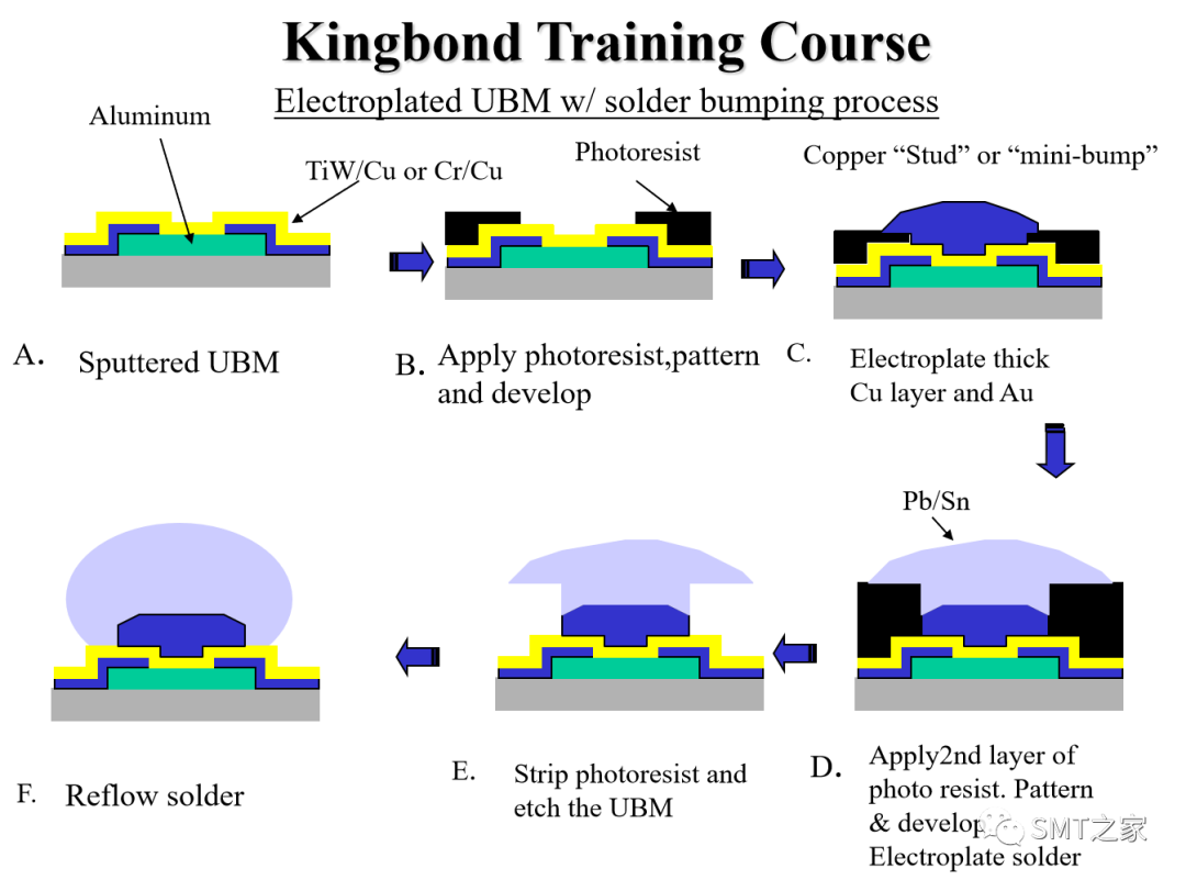
Kingbond Training Course
Flip Chip conductive method - connect to Substrate/PCB
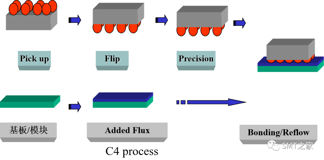
1.Metal bump 金属凸块-C4 process(IBM)
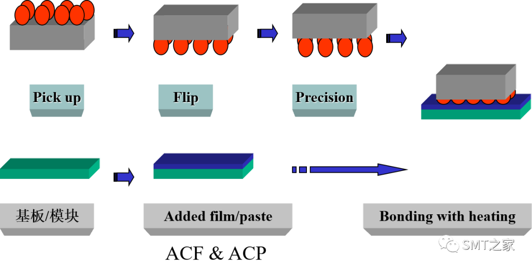
2. Tape-Automated bonding 卷带接合-ACF process
3. Anisotropic conductive adhesives
异方向性导电胶 -ACP process
4.Polymer bump 高分子凸块 - C4 process
5.Stud bump. 打线成球 - ACP process(Matsushita)
C4: controlled collapse chip connection
ACF: anisotropic conductive film
ACP(ACA): anisotropic conductive Adhesive paste
Various flip chip technologies
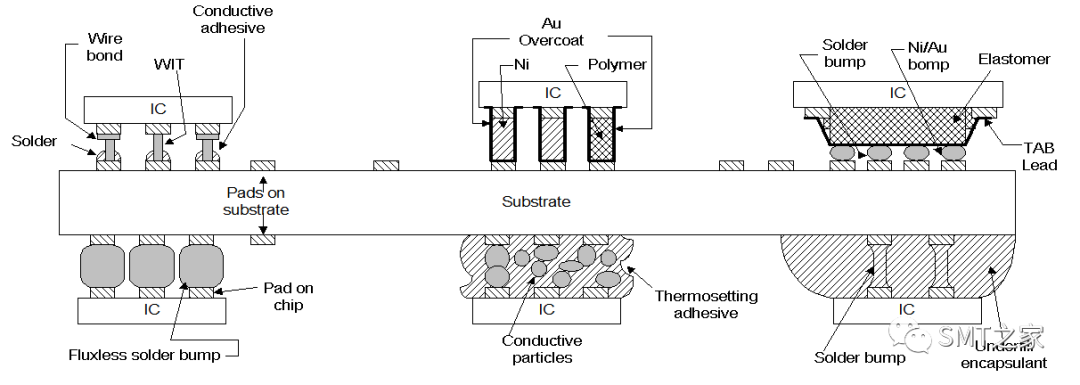
PS: WIT ( Wire interconnect technology)
TAB(Tape- automated bonding)
Various flip chip technologies
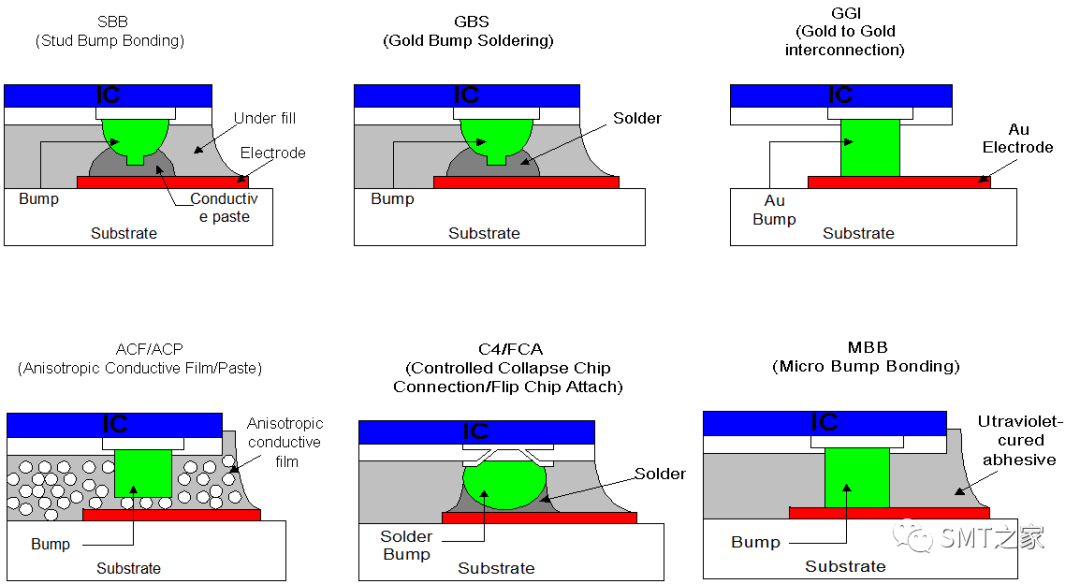
SBB Process
C4: Controlled Collapse Chip Connection Process
ACP: Anisotropic Conductive Paste Process
ACF: Anisotropic Conductive Film Process
Wafer Bump
Metal bump method

1. 蒸镀 Evaporation
2. 溅镀 Sputter
3. 电镀 Electroplating
4. 印刷 Printed solder paste bump
5. 锡球焊接 Solder ball bumping or Stud bump bonding (SBB)
6.无电镀镍 Electroless nickel technologies
Material of solder bump

1.95Sn/5Pb,97Sn/3Pb 高温锡铅合金
2. 63Sn/37Pb 低温锡铅合金
3. Ni 镍
4. Au 金
5.Cu 铜
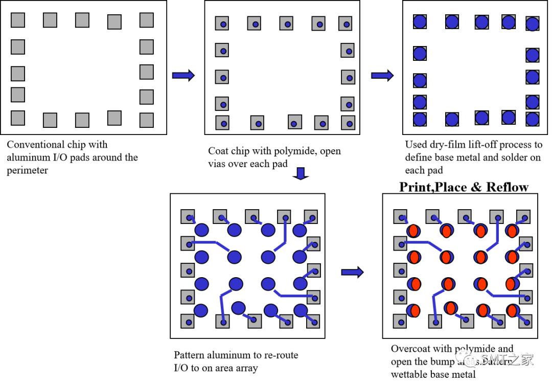
Wafer bump (Printed method) Process:Wafer clean

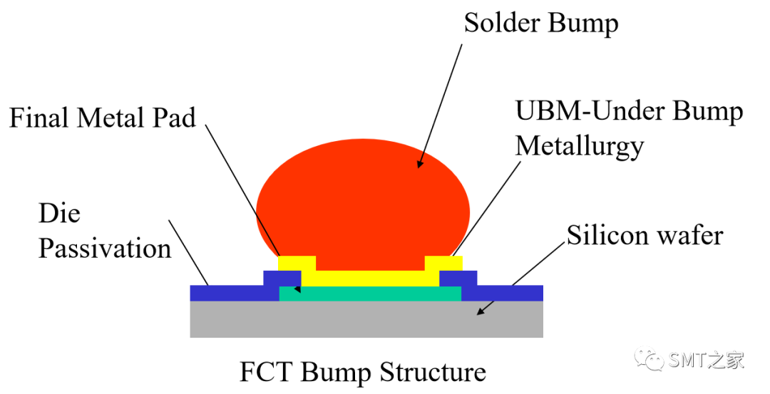
Silicon Wafer arrives with an aluminum based final metal pad and die passivation. Wafer can be probed prior to bumping.
Wafer Bump (Printed method) Process: Sputter UBM
The Under Bump Metallurgy is added by FCT through sputtered layers of Al,Ni-V,&Cu
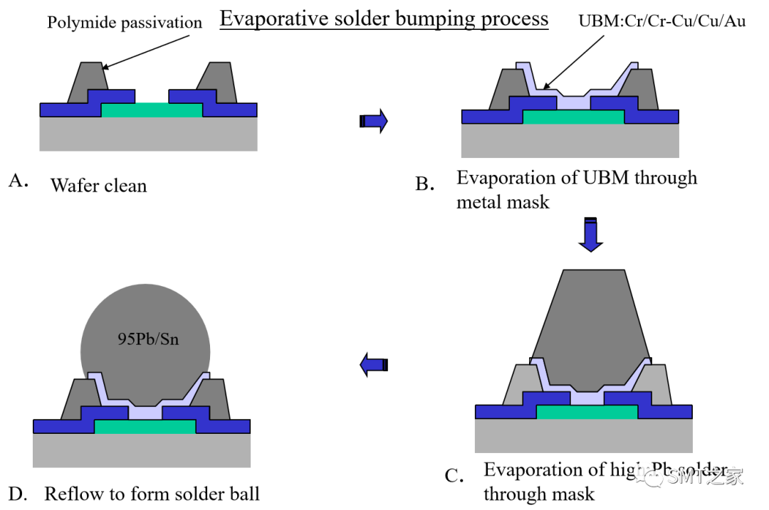
Wafer Bump (Evaporation method)
Process: Sputter UBM
UBM consist 3 layer:
1. Adhesion layer : Ti,Cr,TiW 提供铝垫(Al pad)与护层(Passivation layer)有较强之黏着性
2. Wetting layer:Ni,Cu,Mo,Pt 高温回焊时锡球可完全沾附而成球
3. Protective layer:Au 保护 Ni,Cu等免于被氧化.
Wafer Bump (Printed method)
Process:Photo-resist
Apply photoresist, Pattern and develop
Wafer Bump (Printed method)
Process: Etch UBM

Etch to form UBM cap
Wafer Bump (Printed method)
Process: Print solder paste & reflow

Deposit solder paste and reflow to form bump
Wafer Bump (Printed method)
Process: Inspection

Sample measure bump height, bump shear and bump resistance.
The typical size of a bump before reflow :
1. Evaporative bumps are 125 mils in diameter and 100 mils high.
2. Plated bumps are 125 - 175 mils in diameter and 25 -100 mils high.
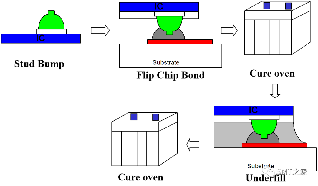
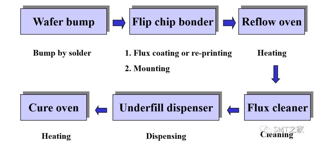
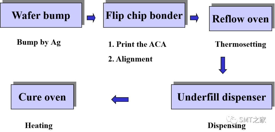
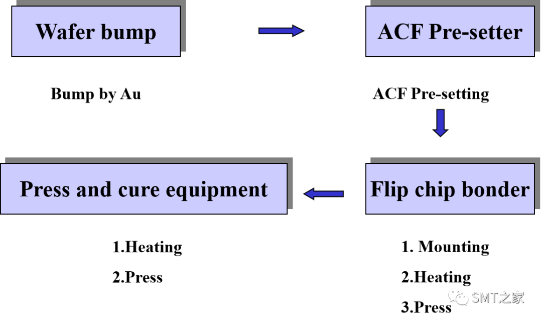
上芯片流程Flip Chip flow
上芯片流程Flip Chip flow
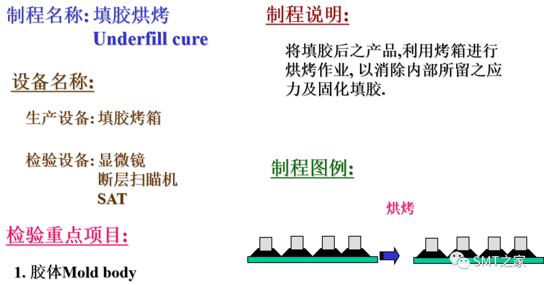
Why do you need to underfill
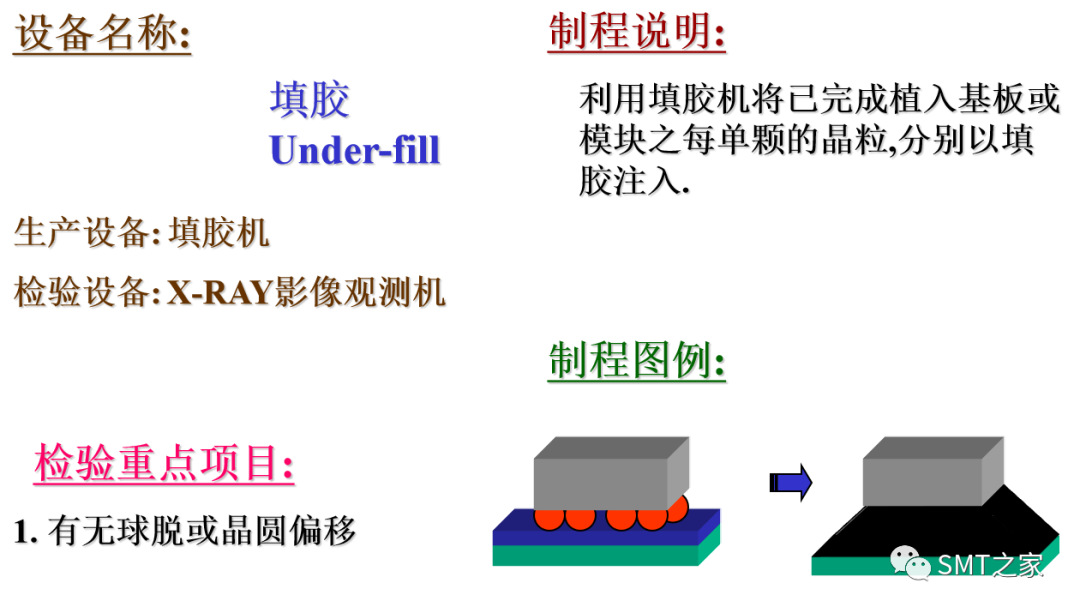
填胶制程 Under-fill
1. 毛细作用型 Capillary type):
利用毛细力造成胶材之流动.
2. 异方向导电胶(Anisotropic conductive adhesive):
低温制程,分膏状(paste)和膜状(film)
3. 前置型(Pre-applied type):
小尺寸芯片(<6mm),点胶(Die attachment)后再回焊(Reflow)
制程与材料之限制:
1. 加强快速填胶与固化能力
2. 提升其界面之黏着力
3. 较低的吸水率
4. 提升低锡铅球间距内的流动性
5. 加强可重工性(rework)
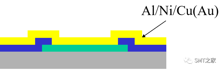
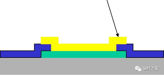
Polymide passivation Evaporative solder bumping process
UBM:Cr/Cr-Cu/Cu/Au
编辑:黄飞
-
半导体“倒装芯片(Flip - Chip)”焊界面退化的详解;2026-02-24 4962
-
寻找珠三角地区能够提供FLIP CHIP,WIRE BOND封装服务的厂家2018-04-02 6388
-
Flip-Chip倒装焊芯片原理与优点2018-09-11 10677
-
allegro中怎么生成flip chip裸die的.DRA文件2022-08-15 51392
-
(Flip-Chip)倒装焊芯片原理2009-11-19 2372
-
倒装焊芯片(Flip-Chip)是什么意思2010-03-04 23312
-
RFID封装工艺:Flip Chip和wire bonding2011-03-04 12222
-
一文详解精密封装技术2022-12-30 2824
-
一文详解分立元件门电路2023-03-27 5392
-
一文详解Flip Chip制程工艺2023-07-25 5453
-
一文详解pcb和smt的区别2023-10-08 6213
-
一文详解pcb的msl等级2023-12-13 17431
-
浅谈芯片倒装Flip Chip封装工艺2024-02-20 4133
-
倒装芯片(flip chip)算先进封装吗?未来发展怎么样?2024-12-02 2723
-
倒装封装(Flip Chip)工艺:半导体封装的璀璨明星!2025-01-03 7537
全部0条评论

快来发表一下你的评论吧 !
