

浅析DDR4信号完整性测试完整内容
存储技术
描述
DDR4信号测试主要分为以下几种情况: 1.以手机为代表的多阶表贴内存颗粒,由于主芯片与内存颗粒几乎是挨着摆放,信号不是通孔,没有测试点,要测试必须使用interposer;
2.以电视为代表的单面表贴颗粒,这种有条件也可以上interposer,没条件就直接刮开过孔、刮开走线绿油测试是一样的。像下面一样,TOP层4mil间距DQS差分焊线,不知道有多少人能做到
3.以PC为代表的UDIMM条,这是最简单的。单面贴的内存条背面都有信号过孔,在过孔处找点测试即可;
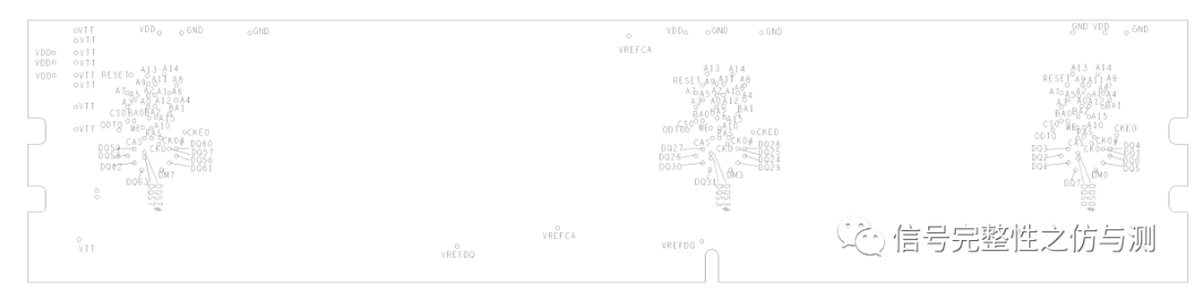
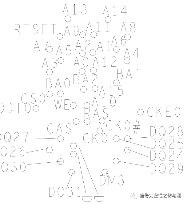
4.以Server为代表的服务器RDIMM,包括笔记本的SODIMM,通常都是双面贴颗粒的,也需要用到interposer;
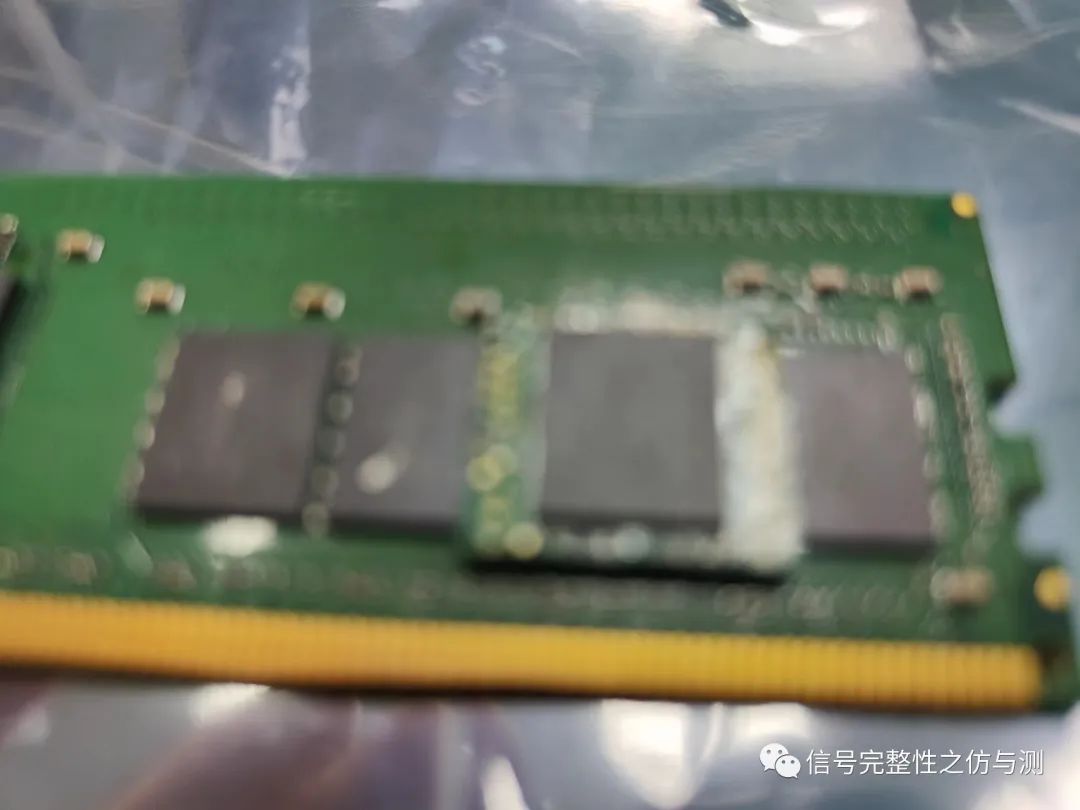
当然还有一种办法,吹掉RDIMM背面的一个颗粒,修改SPD信息,将双面内存修改为单面内存,虽然内存容量降低一半,对于信号测试而言没有什么影响,最重要的是这样就有测试点了,对于主板长走线而言,少一个颗粒的这点分叉影响是微乎其微的,就算上interposer一样也有分叉。亲测有效! 波形读写分离的方法:
通过单次触发得到一个读或者写的波形,读的波形是DQS和DQ的相位是基本相同的。写的波形是DQS和DQ的相位基本上是90度。
触发到单个波形之后,通过以下两种方法来看叠加的波形:
1.通过触发到的波形,利用图形触发(Visual Trigger)选定大体的逻辑区域(in或者out),Kesight示波器是InfiniiScan;
2.通过看读和写的单波形,会发现,读和写DQS的前两个高低电平的宽度是不一样的,使用示波器的宽度(width)触发功能,来触发DQS。
注1:泰克Visual Trigger和是德InfiniiScan都是要单独购买的,这个钱千万不要省,真的非常好用,没有分离不出来的。
注2:DDR3通过前导的正负方向触发读写分离在DDR4无效了,因为DDR4读写前导方向不定,也有可能方向是一样的。
1. DDR4芯片管脚定义描述
DDR4管脚功能描述见下表。
| Symbol | Type | Function | |||
| CK_t, CK_c | Input | Clock: CK_t and CK_c are differential clock inputs. All address and control input signals are sampled on the crossing of the positive edge of CK_t and negative edge of CK_c. | |||
| CKE, (CKE1) | Input | Clock Enable: CKE HIGH activates, and CKE Low deactivates, internal clock signals and device input buffers and output drivers. Taking CKE Low provides Precharge Power Down and Self-Refresh operation (all banks idle), or Active Power-Down (row Active in any bank). CKE is synchronous for Self-Refresh exit. After VREFCA and Internal DQ Vref have become stable during the power on and initialization sequence, they must be maintained during all operations (including Self-Refresh). CKE must be maintained high throughout read and write accesses. Input buffers, excluding CK_t,CK_cS ODT and CKE are disabled during power-down. Input buffers, excluding CKE, are disabled during Self Refresh. | |||
| CS_n, (CS1_n) | Input | Chip Select: All commands are masked when CS_n is registered HIGH. CS_n provides for external Rank selection on systems with multiple Ranks. CS_n is considered part of the command code. | |||
| C0,C1,C2 | Input | Chip ID : Chip ID is only used for 3DS for 2,4,8high stack via TSV to select each slice of stacked component. Chip ID is considered part of the command code | |||
| ODT, (ODT1) | Input | On Die Termination: ODT (registered HIGH) enables RTT_NOM termination resistance internal to the DDR4 SDRAM. When enabled, ODT is only applied to each DQ, DQS_t, DQS_c and DM_n/DBI_n/TDQS_t, NU/TDQS_c (When TDQS is enabled via Mode Register A11=1 in MR1) signal for x8 configurations. For x16 configuration ODT is applied to each DQ, DQSU_t, DQSU_c, DQSL_t, DQSL_c, DMU_n, and DML_n signal. The ODT pin will be ignored if MR1 is programmed to disable RTT_NOM. | |||
| ACT_n | Input | Activation Command Input : ACT_n defines the Activation command being entered along with CS_n. The input into RAS_n/A16, CAS_n/A15 and WE_n/A14 will be considered as Row Address A16, A15 and A14 | |||
|
RAS_n/A16. CAS_n/ A15. WE_n/A14 |
Input | Command Inputs: RAS_n/A16, CAS_n/A15 and WE_n/A14 (along with CS_n) define the command being entered. Those pins have multi function. For example, for activation with ACT_n Low, those are Addressing like A16,A15 and A14 but for non-activation command with ACT_n High, those are Command pins for Read, Write and other command defined in command truth table | |||
|
DM_n/DBI_n/ TDQS_t, (DMU_n/ DBIU_n), (DML_n/ DBIL_n) |
Input/Output | Input Data Mask and Data Bus Inversion: DM_n is an input mask signal for write data.Input data is masked when DM_n is sampled LOW coincident with that input data during a Write access. DM_n is sampled on both edges of DQS. DM is muxed with DBI function by Mode Register A10,A11,A12 setting in MR5. For x8 device, the function of DM or TDQS is enabled by Mode Register A11 setting in MR1. DBI_n is an input/output identifying whether to store/output the true or inverted data. If DBI_n is LOW, the data will be stored/output after inversion inside the DDR4 SDRAM and not inverted if DBI_n is HIGH. TDQS is only supported in X8 | |||
| BG0 - BG1 | Input | Bank Group Inputs: BG0 - BG1 define to which bank group an Active, Read, Write or Precharge command is being applied. BG0 also determines which mode register is to be accessed during a MRS cycle. X4/8 have BG0 and BG1 but X16 has only BG0 | |||
| BA0 - BA1 | Input |
Bank Address Inputs: BA0 - BA1 define to which bank an Active, Read, Write or Precharge command is being applied. Bank address also determines which mode register is to be accessed during a MRS cycle. |
|||
| A0 - A17 | Input | Address Inputs: Provide the row address for ACTIVATE Commands and the column address for Read/Write commands to select one location out of the memory array in the respective bank. (A10/AP, A12/BC_n, RAS_n/A16, CAS_n/A15 and WE_n/A14 have additional functions, see other rows.The address inputs also provide the op-code during Mode Register Set commands.A17 is only defined for the x4 configuration. | |||
| A10 / AP | Input | Auto-precharge: A10 is sampled during Read/Write commands to determine whether Autoprecharge should be performed to the accessed bank after the Read/Write operation. (HIGH: Autoprecharge; LOW: no Autoprecharge).A10 is sampled during a Precharge command to determine whether the Precharge applies to one bank (A10 LOW) or all banks (A10 HIGH). If only one bank is to be precharged, the bank is selected by bank addresses. | |||
| A12 / BC_n | Input | Burst Chop: A12 / BC_n is sampled during Read and Write commands to determine if burst chop (on-the-fly) will be performed. (HIGH, no burst chop; LOW: burst chopped). See command truth table for details. | |||
| RESET_n | Input | Active Low Asynchronous Reset: Reset is active when RESET_n is LOW, and inactivewhen RESET_n is HIGH. RESET_n must be HIGH during normal operation. RESET_n is a CMOS rail to rail signal with DC high and low at 80% and 20% of VDD, | |||
| DQ | Input / Output | Data Input/ Output: Bi-directional data bus. If CRC is enabled via Mode register then CRC code is added at the end of Data Burst. Any DQ from DQ0~DQ3 may indicate the internal Vref level during test via Mode Register Setting MR4 A4=High. Refer to vendor specific data sheets to determine which DQ is used. | |||
|
DQS_t, DQS_c, DQSU_t, DQSU_c, DQSL_t, DQSL_c |
Input / Output | Data Strobe: output with read data, input with write data. Edge-aligned with read data, centered in write data. For the x16, DQSL corresponds to the data on DQL0-DQL7; DQSU corresponds to the data on DQU0-DQU7. The data strobe DQS_t, DQSL_t and DQSU_t are paired with differential signals DQS_c, DQSL_c, and DQSU_c, respectively, to provide differential pair signaling to the system during reads and writes. DDR4 SDRAM supports differential data strobe only and does not support single-ended. | |||
| TDQS_t, TDQS_c | Output |
Termination Data Strobe: TDQS_t/TDQS_c is applicable for x8 DRAMs only. When enabled via Mode Register A11 = 1 in MR1, the DRAM will enable the same termination resistance function on TDQS_t/TDQS_c that is applied to DQS_t/DQS_c. When disabledvia mode register A11 = 0 in MR1, DM/DBI/TDQS will provide the data mask function or Data Bus Inversion depending on MR5; A11,12,10and TDQS_c is not used. x4/x16 DRAMs must disable the TDQS function via mode register A11 = 0 in MR1. |
|||
| PAR | Input | Command and Address Parity Input: DDR4 Supports Even Parity check in DRAMs with MR setting. Once it’s enabled via Register in MR5, then DRAM calculates Parity with ACT_n,RAS_n/A16,CAS_n/A15,WE_n/A14,BG0-BG1,BA0-BA1,A17-A0. Input parity should maintain at the rising edge of the clock and at the same time with command & address with CS_n LOW | |||
| ALERT_n | Input/Output | Alert: It has multi functions such as CRC error flag, Command and Address Parity error flag as Output signal. If there is error in CRC, then Alert_n goes LOW for the period time interval and goes back HIGH. If there is error in Command Address Parity Check, then Alert_n goes LOW for relatively long period until on going DRAM internal recovery transaction to complete. During Connectivity Test mode, this pin works as input. Using this signal or not is dependent on system. In case of not connected as Signal, ALERT_n Pin must be bounded to VDD on board. | |||
| TEN | Input | Connectivity Test Mode Enable: Required on X16 devices and optional input on x4/x8 with densities equal to or greater than 8Gb.HIGH in this pin will enable Connectivity Test Mode operation along with other pins. It is a CMOS rail to rail signal with AC high and low at 80% and 20% of VDD. Using this signal or not is dependent on System. This pin may be DRAM internally pulled low through a weak pull-down resistor to VSS. | |||
| NC | No Connect: No internal electrical connection is present. | ||||
| VDDQ | Supply | DQ Power Supply: 1.2 V +/- 0.06 V | |||
| VSSQ | Supply | DQ Ground | |||
| VDD | Supply | Power Supply: 1.2 V +/- 0.06 V | |||
| VSS | Supply | Ground | |||
| VPP | Supply | DRAM Activating Power Supply: 2.5V (2.375V min, 2.75V max) | |||
| VREFCA | Supply | Reference voltage for CA | |||
| ZQ | Supply | Reference Pin for ZQ calibration | |||
2.测试准备 焊台,植球温控板,DDR,镊子,烙铁,DDR转接板,助焊剂,吸锡带,锡球 测试仪器TEK DSA71254 12.5G 100GS/S 探头:P7313 13G x4或者P7513
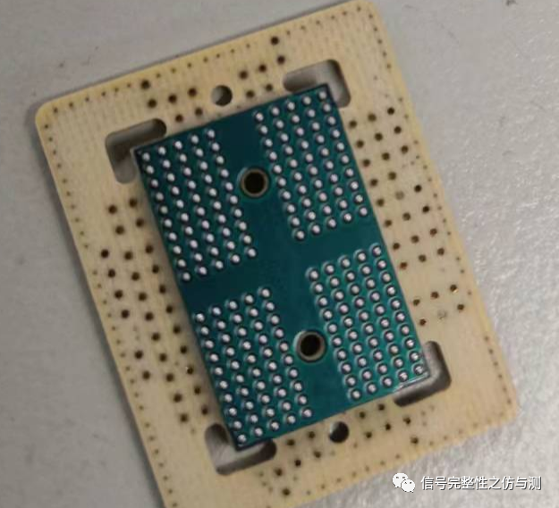
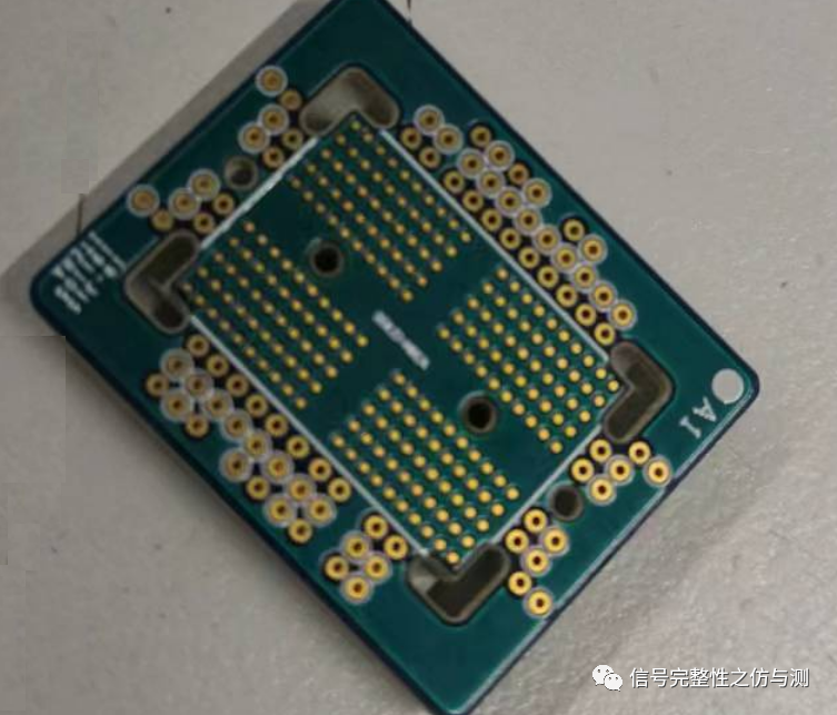
焊接完成如图1-2:
图1-2
3.测试项目分解:
DDR测试主要有以下几个部分:时序的测量,纹波的测量,信号完整性的测量 信号完整性的测量又包括:CLK的测量,CMD&ADD的测量,写操作和读操作的测量。 一般DDR厂家针对DDR的测试只是每个通道选取一颗,每一颗只是测试部分信号,不是全面的测试。如果有条件,想做一个全面的测试。按照下面的测试方法,完全可以做全面的测试,比如下面介绍的测试DQ时,只是测试了DQ0,如果有时间和条件,16根DQ可以全部测试,这样验证的会更加全面,耗费的时间也比较长,这样做的必要性也不大。
3.1时序测量: 时序测量主要测试以下几个项目:
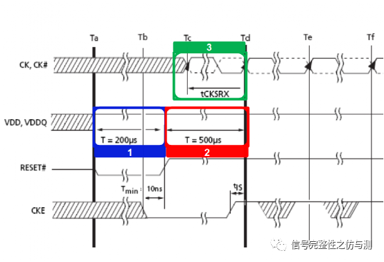
图1-3
VDD to RESET(Reset initialization sequence) 开机后VDD高-reset高 要求:min 200us
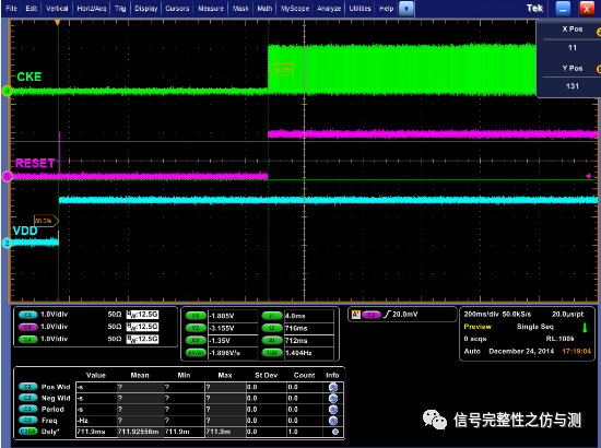
图1-4
RESET to CKE 开机后reset高-CKE使能 要求:min:500us
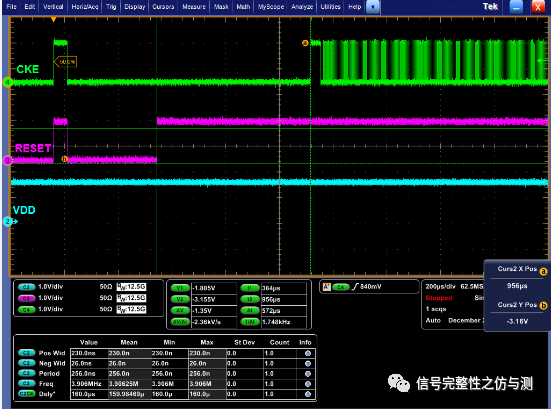
图1-5
tCKSRX CLK稳定到CKE使能 要求 min:5nCK 10ns
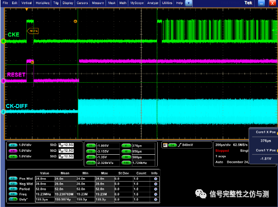
图1-6
Power down模式下才会去测试以下几项:
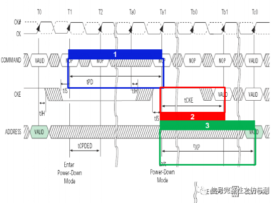
图1-7
tPD power down entry 要求:min: tCKE(min) max:9tREFI
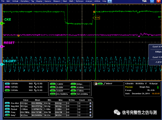
图1-8
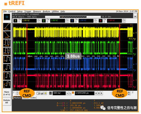
tCKE 要求:min:(max 3nCK,5ns) CKE 高---地址有效 tXP 要求 min:(max 3nCK,6ns) CKE 高---CS有效 tREFI:自刷新间隔时间 不同的温度有不同的要求: 0C
图1-9
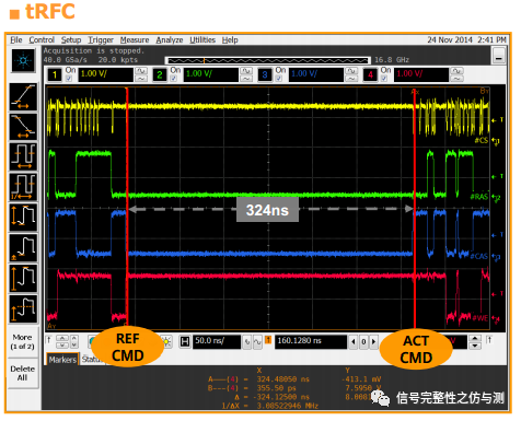
tRFC 自刷新使能时间 要求 min:260ns
图1-10
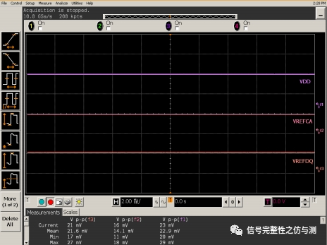
测试自刷新这两个项目的时候,需要使用的触发方式为逻辑触发。设置的逻辑状态为:1 0 0 1. Reset和CKE运行状态确认: 如果不使用PD模式的话,Reset和CKE在正常运行状态下应该都保持高电平 3.2纹波测试: 纹波测试主要测试三个电压的纹波即可。 VDD <75mv VrefCA <=60mv VrefDQ <=60mv 按照正常纹波测试方法测试即可:
图1-11
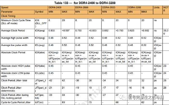
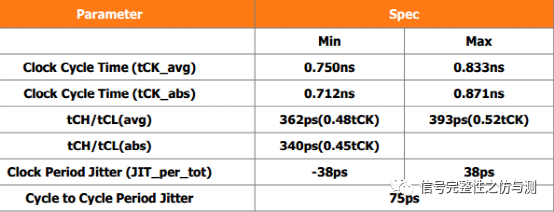
3.3信号完整性的测量: 3.3.1CLOCK相关的测量: Jitter: 与jitter相关的主要有以下几个参数:
以2666速率CLK为例:
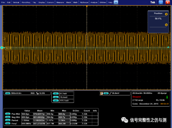
测量jitter时可以手动测量,也可以自动测量。 手动测量要求屏幕内有200个clock,然后添加测量项:pos wid,neg wid,period,freq等。
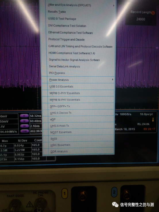
自动测量需要选择示波器的analysis里面的DDR分析功能,需要购买;
进入后需要选择测试的项目: clock,然后选择好clock使用的通道,DDR运行的速率。 设置好以上选项之后,可以一直运行,看看是否会出现有错误的提示。 最后可以导出完整的报告。
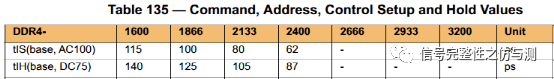
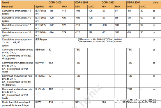
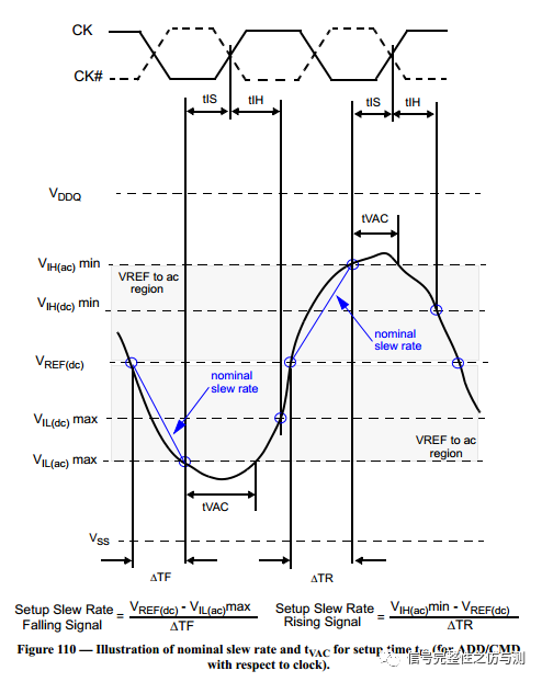
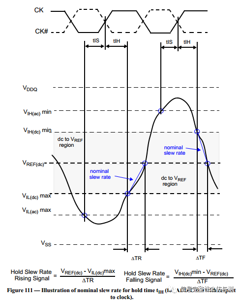
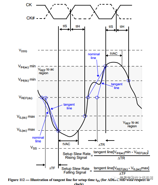
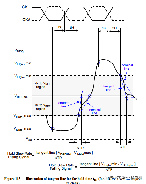
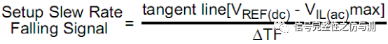
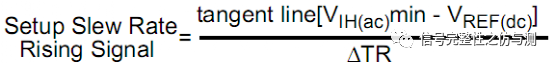
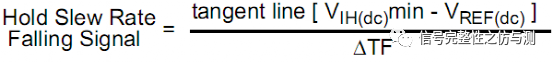
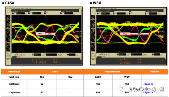
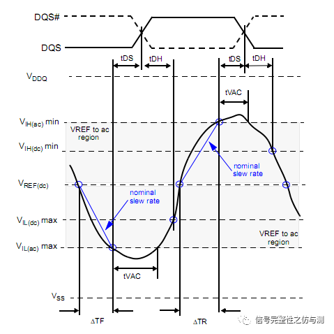
3.3.2命令信号和地址信号的测量: 命令信号和地址信号,一般主要测试CS#,RAS#,CAS#,WE#,ADD,BA,主要测量的是建立时间和保持时间。DDR4和DDR3不同的地方在于,DDR4测试建立时间和保持时间时,不需要再参考斜率了。 tIS>tIS(base) tIH>tIH(base) tIS(base)和tIH(base)都是有对应的值,根据速率不同,定义的值不同。 卡建立时间和保持时间的时候的电平标准是AC100和DC75.
关于CLK-DIFF的计算主要见下图:
Setup的:
Hold的:
Setup非单调的:
Hold非单调的:
测试示例:
TIP:可以将CS信号也放到测试波形中作为参考,因为所有CA信号的选取要参考CS低有效的。
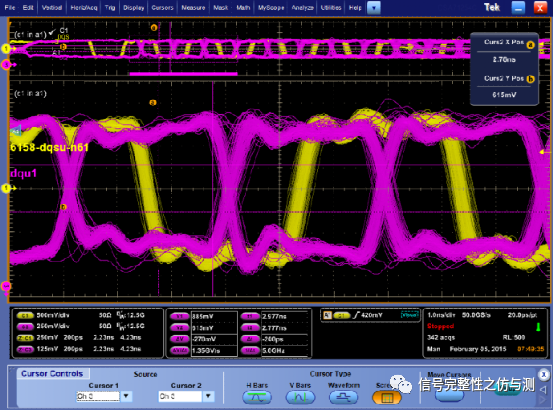
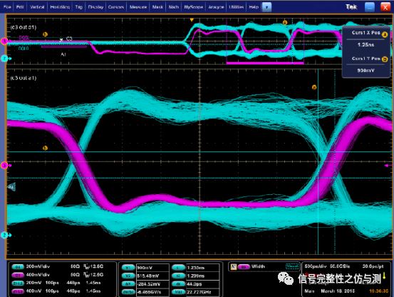
3.3.3写数据的测量: 读数据和写数据的测量都是数据DQ以DQS为参考来做的测量。而不是参照CLK。 DDR4和DDR3在写数据的测量是不同的,DDR3是要测试建立时间和保持时间,而DDR4部分主要是测试眼图。
眼宽和眼高的测试要求如下:
具体波形测量:
写数据的波形
测试示意图:
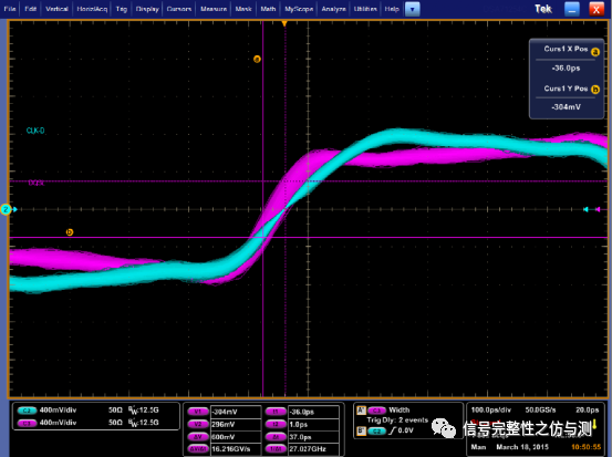
tDQSS为CLK和DQS的相位差,具体测试 波形如下:
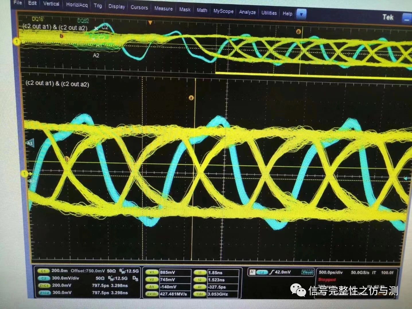
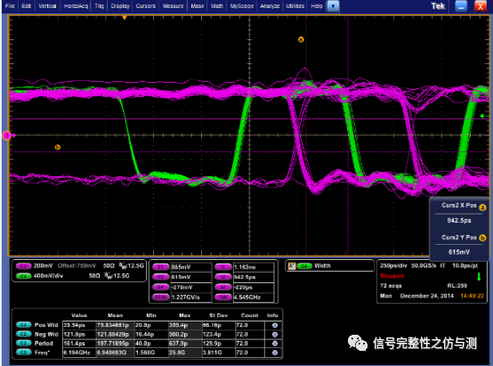
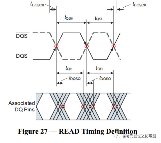
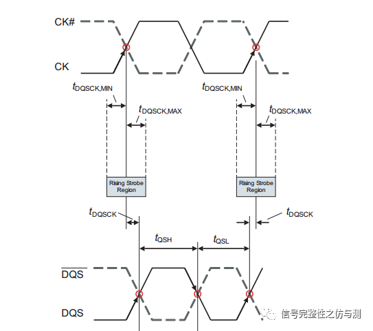
3.3.4读数据的测量: 读数据的测量主要测试的参数有:tDQSQ,tQH,tDQSCK。 测试图示:
tDQSQ要求的值根据DDR运行的速率不同有区别,具体要求见下表:
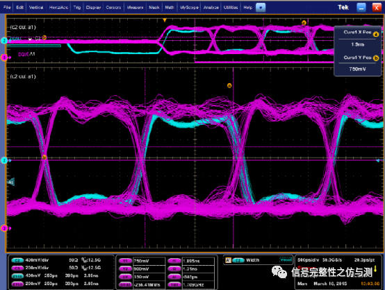
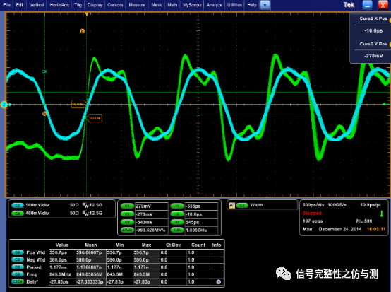
tQH的要求为:min :0.38tCK。 DPO71254测试波形: tDQSQ
tQH
测试中,为了保证测试的准确性,应该多累加测试的波形,这样才能看到整体的波形趋势。
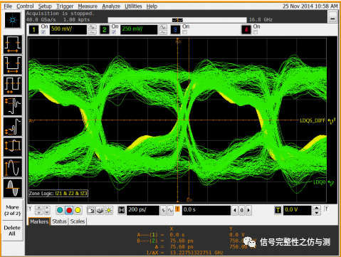
下图为海力士测试波形:
tDQSCK测试的是读数据的CLOCK和读DQS的关系。
测试图示:
参数要求:根据DDR运行的速率不同而不同,具体见下表
DPO71254测试波形:
测试读数据和写数据时,高位与低位的DQ要分别选择一个来测试。
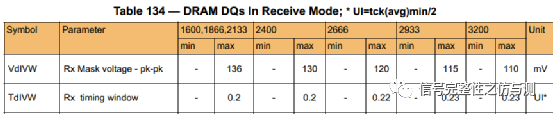
不同速率下各指标要求值范围
不同颗粒厂家新测试项目大同小异,比如三星和海力士:
总结:DDR4测试最好还是选手动测试,手动读写分离很有意思,这样累积波形也看得比较清楚。不需要全测,每种类型抽测即可。自动化软件测试CLK的抖动比较方便,不差钱的话也可以买上;
编辑:黄飞

项目
800
1066
1333
1600
1866
2133
tDQSQ(ps)
min
max
min
max
min
max
min
max
min
max
min
Max
200
150
125
100
85
75
项目
800
1066
1333
1600
1866
2133
tDQSCK(ps)
Min
Max
Min
Max
Min
Max
Min
Max
Min
Max
Min
Max
-400
400
-300
300
-255
255
-225
225
-195
195
-180
180
DDR3 1600
DDR3 1866
DDR3 2133
DDR4 2400
f
[303,800MHz]
[303,933MHz]
[303,1066MHz]
[1066,2400MHz]
tCK(avg)
[1.25,3.3ns]
[1.07,3.3ns]
[0.938,3.3ns]
[0.833,0.938ns]
Duty cycle
[47,53%]
[47,53%]
[47,53%]
[48,52%]
tCH(avg)
[47,53*tCK]
[47,53*tCK]
[47,53*tCK]
[48,52*tCK]
tCL(avg)
[47,53*tCK]
[47,53*tCK]
[47,53*tCK]
[48,52*tCK]
CC Jitter
±140
±120
±100
±83
VIX
[600,900mV]
[600,900mV]
[600,900mV]
[480,720mV]
tDQSS
±0.27tCK
±0.27tCK
±0.27tCK
±0.27tCK
mask
交叉点±70mV, min84ps
三星测试项目
海力士测试项目
类别
测量值
测试要求
测量值
测试要求
CLK(差分)
tCK(avg)
见上表
tCK(avg)
见上表
tCH(avg)
见上表
tCH(avg)
见上表
tCL(avg)
见上表
tCL(avg)
见上表
Duty cycle
见上表
Duty cycle
见上表
Rising Slew
0.4/ck-tR-max
tCK(abs)
tJIT(per)
tJIT(CC)
tCH(abs)
tCL(abs)
CLK(单端)
VIX
MIN:0.5*VDD-0.15/0.12
VIX
MIN:0.5*VDD-0.15/0.12
MAX: 0.5*VDD+0.15/0.12
MAX: 0.5*VDD+0.15/0.12
VSEH
MIN:0.5*VDD+0.175
VSEL
MIN:0.5*VDD-0.175
SLEW RATE
CLK
CLK
CMD&ADD
CMD&ADD
DQS
DQS
DQ
DQ
命令地址CS,RAS, CAS,WE, BA1, AD0,AP, CKE
tIS
tIS
tIH
tIH
Falling Slew
VREF(DC)-VIL(AC)max/ tF
Rising Slew
VREF(DC)-VIL(DC)max/ tR
VIH
AC135
VIL
AC135
Overshoot
Max:0.4
undershoot
Max:0.4
DQ写
DQS rise
tDS DQ高
tDS DQ高
没有单独测上升沿和下降沿,直接选择上升沿和下降沿触发,相当于一次测俩
tDH DQ高
tDH DQ高
tDS DQ低
tDS DQ低
tDH DQ低
tDH DQ低
DQS fall
tDS DQ高
tDS DQ高
tDH DQ高
tDH DQ高
tDS DQ低
tDS DQ低
tDH DQ低
tDH DQ低
DQ
VIH
Vref+0.135
VIL
Vref-0.135
Overshoot
Max:0.4
Undershoot
Max:0.4
DQS
tDQSS
±0.27*tCK
tDQSS
±0.27*tCK
tDSS
MIN:0.18*tCK
tDSH
MIN:0.18*tCK
tDQSH
MIN:0.45*tCK
MAX:0.55*tCK
tDQSL
MIN:0.45*tCK
MAX:0.55*tCK
tWPRE
MIN:0.9*tCK
tWPST
MIN:0.3*tCK
DQ读
DQS
tDQSCK
tDQSCK
tQH
MIN:0.38*tCK
tQSH
MIN:0.4*tCK
tQSL
MIN:0.4*tCK
tRPRE
MIN:0.9*tCK
tRPST
MIN:0.3*tCK
DQS RISE
tDQSQ(DQ rise)
tDQSQ(DQ fall)
DQS FALL
tDQSQ(DQ rise)
tDQSQ(DQ fall)
DQ
VOH(AC)
MIN:0.9
VOL(AC)
MAX:0.6
Overshoot
Max:0.4
Undershoot
Max:0.4
电源
(海力士只测一个颗粒的纹波)
VDD纹波
TBD
VDD纹波
TBD
VrefCA纹波
VDD±2%
VrefCA纹波
VDD±2%
VrefDQ纹波
VDD±2%
VrefDQ纹波
VDD±2%
VDD/Q
MIN:1.425
MAX:1.575
VREF
MIN:VDD(min)(测量值)*0.49
MAX:VDD(max)(测量值)*0.51
时序(海力士只测一个颗粒的时序)
Reset rise to CKE rise
Min:500us
Reset rise to CKE rise
Min:500us
VIH
MIN:0.8*VDD=1.2V
VIL
MAX:0.2*VDD=0.3V
Overshoot
Max:0.4V
Undershoot
Max:0.4V
Reset need to be maintained below 0.2*VDD with stable power
Min 200us
tCKSRX
MIN:MAX(5nCK,10ns)
tREFI
tRFC
-
听懂什么是信号完整性2024-12-15 1481
-
信号完整性与电源完整性-电源完整性分析2024-08-12 3547
-
DDR4信号完整性测试要求2024-01-08 5372
-
信号完整性设计测试入门2023-09-21 3397
-
基于PDN共振峰的最坏情况数据模式分析电源完整性对FPGA DDR4存储器接口中的信号完整性的影响2023-09-13 614
-
什么是信号完整性?2023-06-27 3706
-
信号完整性测试概述2023-02-23 3848
-
信号完整性与电源完整性的仿真2021-09-29 1712
-
信号完整性是什么2021-01-25 2708
-
信号完整性系列之“信号完整性简介”2021-01-23 2637
-
信号完整性系列之信号完整性简介2021-01-20 2651
-
怎么进行兼顾电源影响的DDR4信号完整性仿真2021-01-08 1516
-
信号完整性与电源完整性仿真分析2011-11-30 2162
-
信号完整性原理分析2009-11-04 1314
全部0条评论

快来发表一下你的评论吧 !
