

逻辑综合概述和工艺库详解
电子说
描述
本节主要介绍:
逻辑综合概述
计算延时模型
综合目标
综合流程
综合基本命令
工艺库及其综合库
逻辑综合概述
DC工作流程主要分为四步:
synthesis = translation + Constrain + logic optimization + gate mapping
Translation :翻译功能,主要把RTL级的代码,首先通过转换器GTECH将代码转换成统一用门级描述的电路(Generic Boolean Gates)或者没有映射的ddc格式;
Constrain :加载约束,设置时钟频率,输入延迟,输出延迟,负载,工作电压等
Logic optimization :逻辑优化, 用统一的门级描述电路对面积和时序进行优化。
Gate mapping :门级映射,dc用工艺库厂商的工艺库把电路给映射成基本单元,工艺库包括不同触发器、逻辑门等标准单元,不同类型的标准单元驱动能力和延迟均不同;在约束文件的作用下,DC编译出的网表可以符合特定场景下的功能要求,最终得到一个.ddc文件;
.ddc文件包含许多丰富信息,如映射的门电路信息与网表、寄生参数、.v的网表、SDF标准延时信息、SDC约束、工作条件等信息。
吐出的网表文件,SDF延迟文件,并将其反标,可以用于做后仿。
计算延时模型
线负载延迟模型:根据连线挂载的负载数量进行计算;
拓扑结构模型:通过物理约束(phy)和物理库(lib),给dc工具提供大概布局,得出延迟,比较精确;
一般流程是,dc先综合一版,用dc吐出的第一版信息,给后端做一版初步布局,利用ICC工具吐出的物理约束(包括某些器件的大概位置),DC启动拓扑结构模式,利用布局信息再进行综合,这样计算得到的延迟信息比较准确。
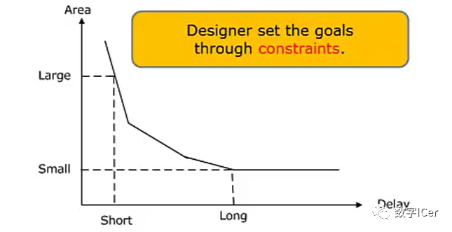
综合目标
面积越小,速度越快;
通常在面积和延时之间折中,如果时序和面积不能同时实现,时序拥有更高的优先级。
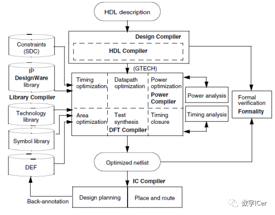
综合流程
综合时,首先DC的HDL compiler把HDL代码转化成DC自带的GTECH格式,然后DC的library compiler 根据标准设计约束(SDC)文件、IP-DW库、工艺库、图形库、(使用拓扑模式时,加入的ICC生成DEF模式,加载物理布局信息)进行时序优化、数据通路优化、功耗优化(DC的power compiler进行)、测试的综合优化(DC的DFT compiler),最后得到优化后的网表。
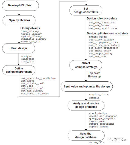
综合基本命令
工艺库
工艺库目录:/opt/Foundary_Library/SMIC_180/smic_180/SM00LB501-FE-00000-r0p0-00rel0/aci/sc-m/synopsys
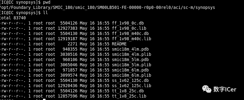
其中:以ss_1v62_125c.lib,ss_1v62_125c.db为例:
.db文件是给DC读取,对应的.lib文件是供人参考;
Library Compiler工具可将.lib文件转换为.db文件;
ff最快工艺工艺角,ss最差工艺角,tt典型工艺角(fast、、slow、typical工作模式)
1v62电压1.62V,125c温度125摄氏度。
电压越低速度越慢,温度越高速度越慢。
打开ss_1v62_125c.lib文件:
版本信息和日期:
  /* documentation attributes */
  revision : 1.0;
  date : "Thu Oct 27 1608 2005";
  comment : "Copyright (c) 2005 Artisan Components, Inc.  All Rights Reserved.";
单位信息:时间、电流、电压、电阻、漏电功耗和负载电容单位信息
  /* unit attributes */
  time_unit : "1ns";
  voltage_unit : "1V";
  current_unit : "1mA";
  pulling_resistance_unit : "1kohm";
  leakage_power_unit : "1pW";
  capacitive_load_unit (1.0,pf);
工作环境:温度、电压
  /* operation conditions */
  nom_process     : 1;
  nom_temperature : 125;
  nom_voltage     : 1.62;
  operating_conditions(ss_1v62_125c) {
    process : 1;
    temperature : 125;
    voltage : 1.62;
    tree_type : balanced_tree
  }
  default_operating_conditions : ss_1v62_125c;
缩放因子:当温度变化时,根据缩放因子做出调整
 /* threshold definitions */
  slew_lower_threshold_pct_fall : 30.0;
  slew_upper_threshold_pct_fall : 70.0;
  slew_lower_threshold_pct_rise : 30.0;
  slew_upper_threshold_pct_rise : 70.0;
  input_threshold_pct_fall      : 50.0;
  input_threshold_pct_rise      : 50.0;
  output_threshold_pct_fall     : 50.0;
  output_threshold_pct_rise     : 50.0;
  slew_derate_from_library      : 0.5;
默认属性:工艺库的最大电容、最大扇出、输入输出电容、漏电功耗等信息
  /* default attributes */
  default_leakage_power_density : 0.0;
  default_cell_leakage_power : 0.0;
  default_fanout_load : 1.0;
  default_output_pin_cap : 0.0;
  default_inout_pin_cap : 0.0035;
  default_input_pin_cap : 0.0035;
  default_max_transition : 4.5;
查找表:计算延迟
  /* templates */
  lu_table_template(delay_template_7x1) {
    variable_1 : input_net_transition;
    index_1 ("1000, 1001, 1002, 1003, 1004, 1005, 1006");
  }
  power_lut_template(energy_template_7x1) {
    variable_1 : input_transition_time;
    index_1 ("1000, 1001, 1002, 1003, 1004, 1005, 1006");
  }
工作电压: GENERAL、CMOS、TTL
  /* pad attributes */
  output_voltage(GENERAL) {
    vol : 0.4;
    voh : VDD - 0.4;
    vomin : -0.5;
    vomax : VDD + 0.5;
  }
  input_voltage(CMOS) {
    vil : 0.3 * VDD;
    vih : 0.7 * VDD;
    vimin : -0.5;
    vimax : VDD + 0.5;
  }
  input_voltage(TTL) {
    vil : 0.8;
    vih : 2;
    vimin : -0.5;
    vimax : VDD + 0.5;
  }
线负载模型:单位电阻,单位电容,斜率,面积,扇出
/* wire-loads */
  wire_load("smic18_wl20") {
    resistance : 8.5e-8;
    capacitance : 1.5e-4;
    area : 0.7;
    slope : 133.334;
    fanout_length (1,133.334);
  }
基本单元:加法器
cell (ADDFHX1M) {
  cell_footprint : addfh;
  area : 59.270400;
  pin(A) {
    direction : input;
    capacitance : 0.006299;
  }
  pin(B) {
    direction : input;
    capacitance : 0.012002;
  }
  pin(CI) {
    direction : input;
    capacitance : 0.004209;
  }
  pin(S) {
    direction : output;
    capacitance : 0.0
    ...
    ...
}
综合库
synthetic_library一般为synopsys的库:DesignWare library 和标准单元库;DesignWare library 为synopsys的IP库:
当使用到synopsys公司的IP核时,则需要定义此综合库;
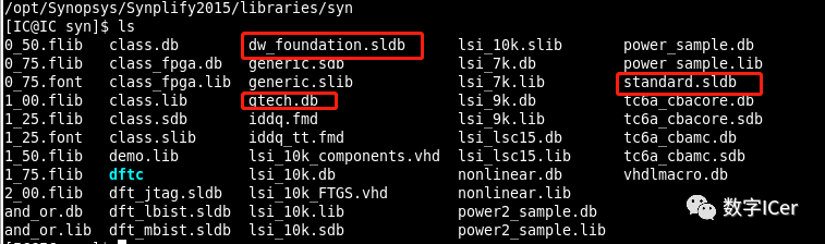
目录:/opt/Synopsys/Synplify2015/libraries/syn:
审核编辑:汤梓红
-
【「龙芯之光 自主可控处理器设计解析」阅读体验】--LoongArch逻辑综合、芯片设计2026-01-18 1053
-
半导体制造工艺之光刻工艺详解2023-08-24 3609
-
逻辑综合的相关知识2023-03-30 1980
-
逻辑综合与物理综合2022-11-28 4073
-
芯片设计之逻辑综合过程2022-08-12 4818
-
什么是逻辑综合?2021-11-02 3437
-
DC逻辑综合详解2021-07-29 1256
-
FPGA的逻辑仿真以及逻辑综合的一些原则2020-05-15 4419
-
逻辑漏洞之越权详解2017-09-07 1031
-
PCB工艺流程详解2013-05-22 10257
-
浅谈IC设计中逻辑综合2013-05-16 6068
-
【参考书籍】XILINX可编程逻辑器件设计技术详解—何宾著2012-04-24 10444
-
DC逻辑综合2011-12-29 924
-
射极耦合逻辑(ECL)基础知识详解2009-08-07 3927
全部0条评论

快来发表一下你的评论吧 !
