

AMD硅芯片设计中112G PAM4串扰优化分析
EDA/IC设计
描述
编者注:在前面我们介绍了很多次PAM4的设计和仿真。在当前高速设计中,主流的还是PAM4的设计,包括当前的56G,112G以及接下来的224G依然还是这样。突破摩尔定律2.5D和3D芯片的设计又给高密度高速率芯片设计带来了空间。本文是AMD在硅芯片设计互连中对112G PAM4的串扰优化的分析介绍。仅供参考。
CrosstalkNoise Optimization for Robust 112G PAM4 Design in StackedSilicon Interconnect Technology
作者:AMD - Leon Chen ,Jinsung Youn, Youngsoo Lee, Po-Wei Chiu,Tianyu (Alan) Fang, Po-Chiao (Joe) Chang
Abstract
2.5D IC with high-density and high-speed capability provides an indispensable solution for datacenter applications by breaking through Moore's law. To achieve a robust 2.5DIC design, there are various electrical design challenges, particularly theintegral part is a healthy channel design in terms of insertion and reflectionlosses, and crosstalk noises to support over one hundred gigabit datatransmission. In this paper, we focus on design parameters related to thecrosstalk noises and optimize the parameters to achieve 112G PAM4 by havingrobustness and channel healthiness. We analyze channel characteristics of a siliconinterposer, a package,and a board in frequencyand time domain,and improve each portion aswell as the entire crosstalk performance based on case studies. With thecrosstalk noise optimization, we can eliminate potential design issues in thedesign stage which can help to reduce turnaround time to debug our 2.5D IC system.
Introduction
As the required data throughput explosively increases in data center and networkingapplications, it needs a cutting-edge system integration which supports highdensity and high bandwidth as well as low-power consumption [1]. Two pointfive-dimensional integrated circuit(2.5D IC) with an advanced packagingtechnologies can be a solution to meet those requirements. However,the 2.5D IC usually faces design challenges because it includescrowded signal routings and power planes and has a vertically stacked configuration with a smallform factor. Thus, from a channel designpoint of view, it could have high insertion and return losses as well as crosstalk noises. Amongthem, mitigating crosstalk noises is particularly challenging because it isrelated to several factors. For example, to meet form factorrequirements, 2.5D IC has dense signal routingsin the silicon interposer, package, and board which can make thecapacitive and inductive coupling. In addition to that, to achieve over one hundred gigabit datatransmission with better energy efficiency, 2.5D IC systems use lower supplyvoltage with multi-level signaling such as pulse amplitude modulation 4-level(PAM4). In case, timing and voltage marginare fairly tight, therefore even small crosstalknoises can degradethe overall signal-to-noise ratio and bit-errorrate [2].
Crosstalk noise is mainlygenerated by both inductive and capacitive coupling of the electromagnetic (EM)field. In the case of receivers, crosstalk noise behaves as wideband noise which cannotbe effectively compensated by equalization in a siliconchip. Moreover, high insertion loss associated with a high-density package squeezes the marginbetween insertion loss and cross-coupling additionally. In addition, as part ofa total link budget, the advanced package usually allows to attenuate no morethan 2.5 dB at either transmitter or receiver and to couple larger than -50 dBnoise aggregately among all transmitting lanes [3].
In thispaper, we investigate design parameters that could affect far-/near-endcrosstalk (FEXT/NEXT) noises for multi-gigabit transceivers, especially 112G PAM4 in
2.5D IC, and then we optimize designparameters based on case studies. The 2.5D IC is composed of a silicon (Si)interposer including through-silicon vias (TSVs), an organic package, and a PCBboard. Micro-bumps (μbumps), controlled collapse chip connection (C4) bumps,and ball grid arrays (BGAs) are placed ateach boundary. There is a rangeof factors that affectthe crosstalk mechanismsuch as C4 bump/BGA map, trace-via coupling, signal trace quality, etc.,thus, we deep dive into those design parameters. To break down each effect, wecreate EM models of the Si interposer, package, and board, and analyze themusing a full-wave EM solver in frequency and time domain. It should be notedthat mechanisms investigated in the paper go beyondcommonly known causes.We identify the advanced crosstalk mechanism and peeloff precisely the individual contribution of each type to the jitter margininside and around a very high-speed design.
One of crosstalk mechanismis a package-PCB breakout coupling.The mechanism is coming from inductivecoupling due to cylinder structures with BGA balls and extended PCB vias underneath. We analyze the different BGA templates and arrangements for FEXTnoises. The other mechanism is a verticalstructure to horizontal trace coupling [4]. It is the
internal effect in the package and PCB whichare originated from the via to signal trace. Those crosstalk noises can cause an excessive jitterin transmitter side. Then, based on case studies, we compare the effect below 28 GHz which is a Nyquistfrequency of 112G PAM4.
Besides, we propose an efficient and practical simulation flow to sign-offproducts. The main challenging point isto have a reasonablesimulation and verification time while keeping the same simulation accuracy. This paperproposes a simulation methodology to save a simulation runtime. Firstly, for anadvanced Si interposer, the meshed power and ground plane are efficientlymerged and sanitized. Then, for an advanced package which has abundant channels, package design issimplified to analyze them in a short time. For multilayer PCB, a hybridsimulation combining 2.5D and 3D simulators providesimulation efficiency. After the design flow and methodology areoptimized, we establish and offer an effective, a well-controlled, and a definitive low-cost solution for identified high-speed applications. We believe thatour crosstalk investigation can provide good an insight to achieve a robust2.5D IC design, and especially it helps to eliminate crosstalk risk factors in the design stage. For system design engineers, thispaper becomes practical to refer to because all crosstalk phenomena andmitigations are studied in real 28 Gbps long reach and mixed long and shortreach links.
Advanced 2.5D-Integrated FPGA System Design
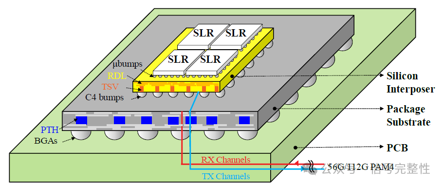
Fig. 1. Conceptual blockdiagram of 2.5D-integrated FPGAsystem design.
Fig. 1 describes aconceptual block diagram of a 2.5D-integrated FPGA system design which iscomposed of field programmable gate array super logic regions (FPGA SLRs), a Siinterposer, an organic package, and a printed circuit board (PCB). For high-speed serializer and de-serializer (SerDes) interface, the FPGA SLRs including SerDes IP are flip-chipped to the Si interposer using micro-bumps (μbumps),and the Si interposer is attached to the packagesubstrate using C4 bumps. The Si interposer contains high-speed SerDes signaltraces and meshed power planes with three metal layers and one thick aluminum metal layer,and those signal nets and powerplanes reach to the C4 bumps with through-silicon vias (TSVs). The multi-layer packageincluding ground reference layers is attached to the PCB with the BGA solderballs. The package includes high-speed SerDes differential pairs which are connected from C4 bumps to BGAs using signal routing layers and plated-through hole (PTH)vias. Then, the SerDes signalnets are routedinside the PCB with striplines from BGAs to SMAconnectors to communicate with other systems.
In this paper, one SerDesquad is focused because the modularized SerDes quad isrepeatedly used inside SLR to support multiple SerDes interfaces. The SerDesquad contains four TX channelsand four RX channels to transmit and receive data fromFPGA to other FPGAs or systems.We evaluate the SerDes TX and RX channel’s crosstalkat both 14 and 28 GHz whichis Nyquist frequency for 56 and 112 Gbps PAM4, respectively.
Co-Design and Co-Simulation Methodology
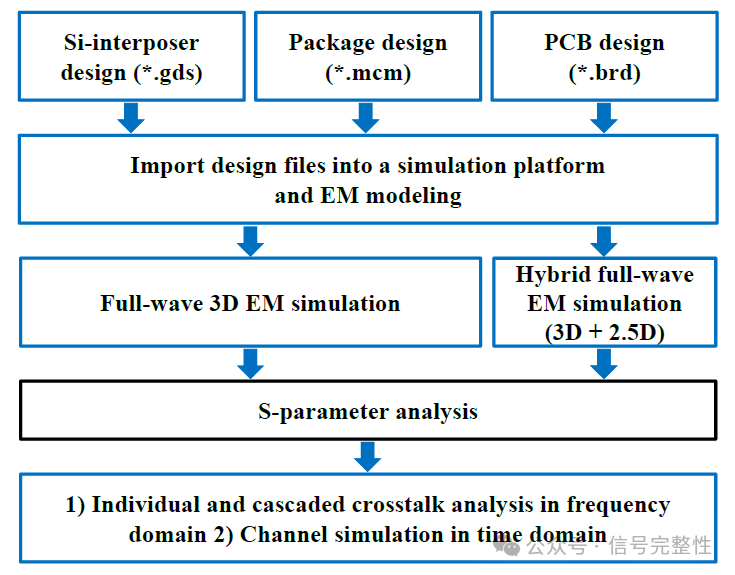
Fig. 2. Co-design and co-simulation methodology for 2.5D IC FPGA.
Fig. 2 shows the co-designand co-simulation methodology for a 2.5D IC FPGA system including Si interposer, package, and PCB. Their physical design filesare directly imported into a simulation platform and defineda layer stack-up, material properties, ports, etc. for EM modeling.Then, each EM model is individually analyzedwith a full-wave EMsimulator. For PCB, we adopt a hybrid simulation method to save simulation timeby mixing a 3D full-wave simulator(e.g., Ansys HFSS 3D Layout)for the vertical part (e.g.,vias) and a 2.5D full-wave simulator (e.g., Ansys SIwave) for horizontalrouting (e.g., signal traces). Compared to the pure 3D full-wave EM simulation,the hybrid simulation saves 84% simulation time (from 45 hrs to 7.2 hrs) foranalyzing four TX and four RX differential pairs with less than 0.2 dB difference in terms of insertion and return lossesas well as crosstalknoises. Then, individual and cascaded crosstalkperformance is analyzed in both frequency and time domainusing a circuit simulator (e.g.,Keysight ADS) with theextracted S-parameters.
To clarify a boundaryeffect at each joint (e.g., Si interposerand package, package and PCB) [5], we compare the cascaded S-parameter extracted from individual EM models with the S-parameter extracted from launched EM models (e.g.,Si interposer plus package,package plus PCB). For this comparison, two launched models were developedbecause it was not allowed to launchall three designs in a row. Thefundamental reason is that there is a large gap in terms ofaspect ratio. Especially, as the Si interposerthickness is too thin than others,it requires immensecomputing and memoryresources and simulation runtime. Each launched structurerequires almost 2-3 weeks simulation time to sweepup to 50 GHz, but only few days are neededif we run the simulation separately. However, the simulationresult difference between the cascadedS-parameter and launchedS-parameter is only 2.1% and 0 % in terms of the FEXT and NEXT at 28 GHz, respectively. Thus, we choose thecascaded model approach in order to save simulation time.
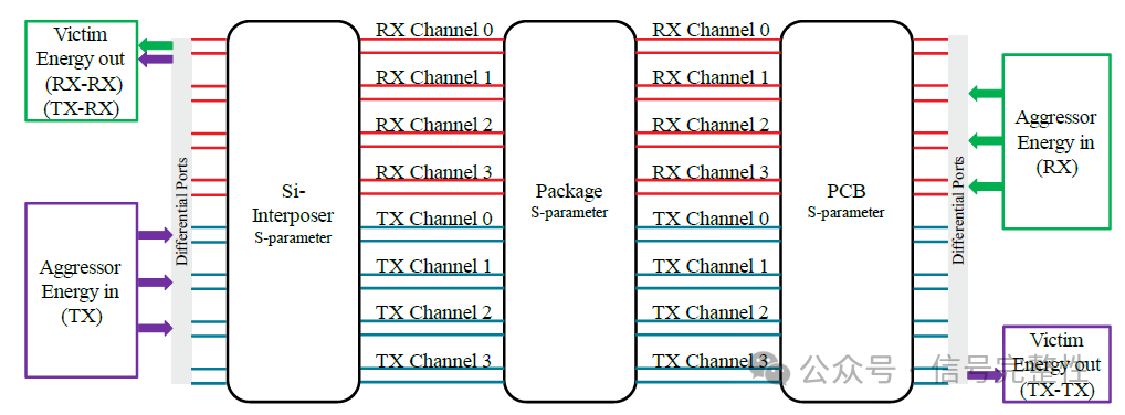
Fig. 3. Schematic diagramfor power sum FEXT and NEXT analysis.
The crosstalk occurs when electrical and magnetic fieldsfrom one differential pair interfere adjacent differential pair, which results inunwanted electrical and magnetic energy coupling. The active differential pairsare called aggressors, and the quiet differential pairs are named victims. When signal travelsthrough the aggressor line, it willencounter the effective mutual inductance and capacitance between theaggressors and victim which also changes the voltage. The direction of theunwanted coupling current generated from the capacitive couplingdepends on the impedance of the current’s side and thedirection of the inductive coupling which is chosen by Lenz’s law.
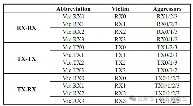
Fig. 3 depicts schematicdiagrams for defining TX-TX and RX-RX FEXT as well as TX-RX NEXT with thecascaded S-parameter of Si interposer, package, and PCB. As we focus on and extract one SerDes quad, each S-parameter has 16 ports to define four TX and four RX differential pairs. Eachpair of channels is converted into differential and common mode by using the ideal balun function in the circuitsimulator. The definition of the power sum FEXT (PSFEXT) TX-TX is the summation of the crosstalk energy from the threeaggressors entering from the μbumpsto the end of connectors, and the remaining TX channel is the victim. The PSFEXT RX-RX has an opposite directioncompared to TX-TX, that is, from connectors toμbumps. For the definition of power sum NEXT (PSNEXT) TX-RX, the aggressor energy from TX is inserted to μbumps, and measured energy at RX victim channel at μbumps. The details of the victim and aggressors are presented for each TX-TX, RX-RX, andTX-RX cases in Table 1.
Table 1. Definition of the victimand aggressors for each crosstalk case
Crosstalk Noise Optimization for Robust 112G PAM4
A. Far-End Crosstalk of RX-RXand TX-TX
This section focuses onthe RX-RX and TX-TX crosstalk. Fig. 4(a) and (b) show PSFEXT RX-RX including differentvictim cases at 14 and 28 GHz, respectively. In both plots, the green, blue, purple, andblack lines represent PSFEXT RX-RXof Si interposer, package, PCB, and the cascaded case. Fig. 4(c)-(f) summarizesthe detailed wave format in the frequency domain for each victim case.The graphs show that the cascaded PSFEXT RX-RX is mainly restricted by the Si interposer. Also,as referring to channel 1 and 2, PCBdesign influences the PSFEXT RX-RX as well. Fig. 5(a) and (b) illustrates thePSFEXT TX-TX of Si interposer, package, PCB, and the cascaded result, and thedetailed wave formats are in the Fig. 5(c)-(f). Compared to the PSFEXT RX-RX,the Si interposer does not dominate the crosstalk as TX channel spacing isfarther than RX channel spacing. Instead, for PSFEXT TX-TX, the PCB almostcontrols the entire system-level crosstalk performance. One of the reasons forthis phenomenon is that TX signals inside PCB are mainly routed with relativelydeeper layers than RX signals. Therefore, TX signals can have more verticalmutual coupling than RX signals. We investigate design optimization of Si interposer and PCB to reduce the PSFEXT RX-RXand TX-TX, it is presentedin the following subsections.
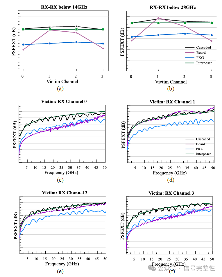
Fig. 4. PSFEXTRX-RX below (a) 14 and (b) 28 GHz.Simulated S-parameter plotswhen the victim is RX (c) ch0, (d) ch1, (e) ch2, and (f) ch3,respectively.
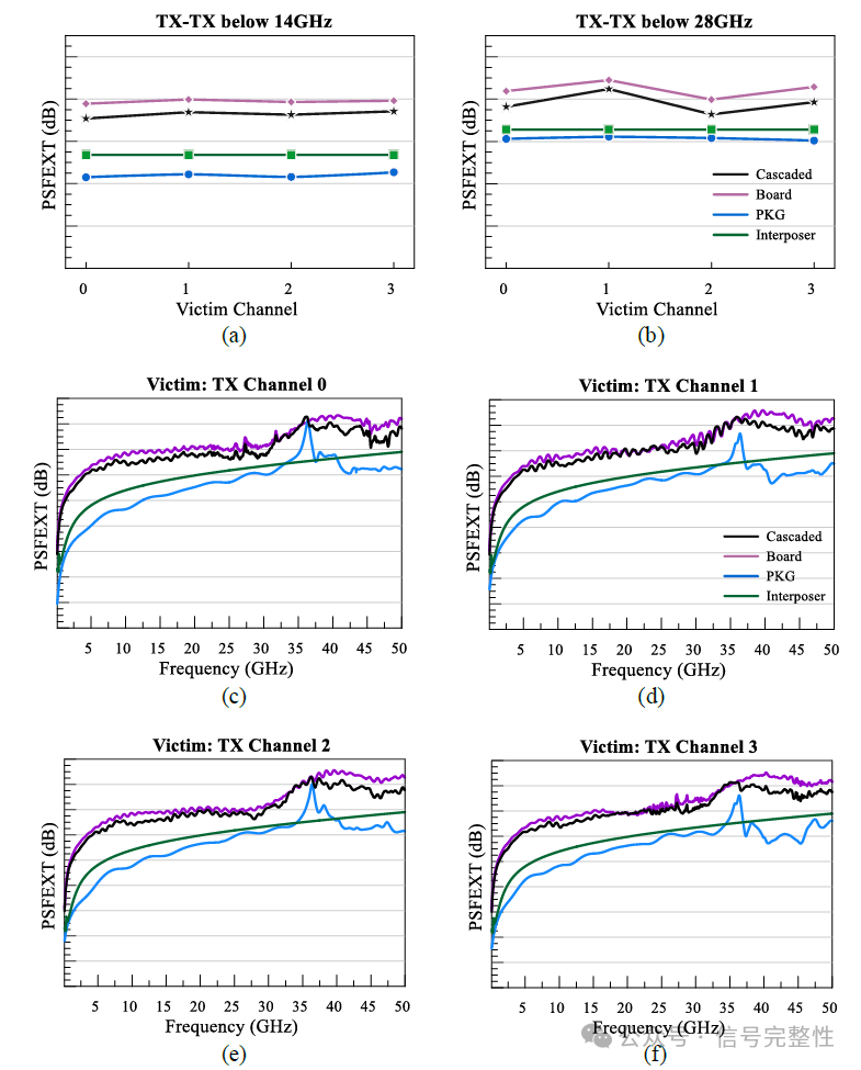
Fig. 5. PSFEXT TX-TXbelow (a) 14 and (b) 28 GHz. Simulated S-parameter plots when the victim is TX (c) ch0, (d) ch1,(e) ch2, and (f) ch3, respectively.
1)Silicon Interposer
The Si interposer is a delicatedesign which has many meshed patterns, and a bunch of small vias that can cause a long simulation time and huge memory resources, therefore, an efficient EM modeling approachis essential. After importing the Si interposer GDS file into a full-wave simulator, the Si interposer design is simplified by unifying and sanitizingthe meshed power and groundplanes as well as by merging via structure. As shown in Fig.6, in this work, the simplified Si interposer layout includesone SerDes quad (i.e., four TXand four RX pairs). The SerDes signalsare directly connected with stacked via from μbump to C4 bump. As can be seen in Fig. 6, TX’s minimumchannel-to-channel distance ”A” is larger than RX’s minimum distance “B”. Basically, the crosstalk islimited by the nearest channel,PSFEXT TX-TX when TX0 is the victim shows an 24 % lower crosstalk level thanPSFEXT RX-RX when RX0 is the victim as shown in the Fig. 7(a).
One way to optimizePSFEXT RX-RX is increasing channel-to-channel distance as the TX. To investigate a relationship of PSFEXT versusa distance, PSFEXT at 28 GHz ismeasured with different distances and plotted as shown in Fig. 7(b). Withincreasing the channel-to-channel distance, PSFEXT is gradually improved. Fromthis graph, the C4 bump floorplan can be determined to meet the specific PSFEXTlevel. Also, we investigated the effect of the ground shield after removing theground guarding, the PSFEXT decreased by almost 5 % due to the worse isolation.Thus, a ground guarding should be inserted for better crosstalk performance.
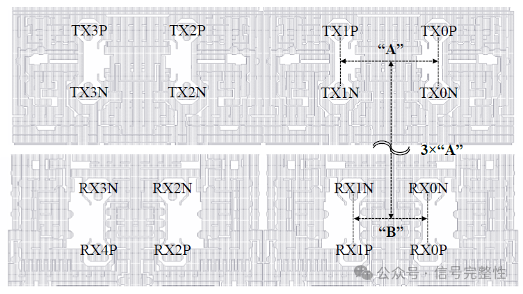
Fig. 6. Si interposer layout
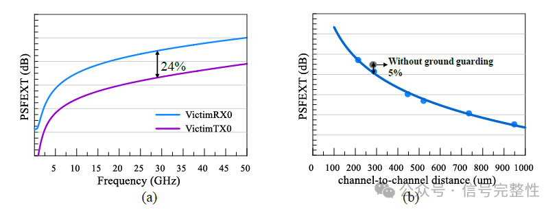
Fig. 7. (a) Comparison of PSFEXT TX-TX and RX-RX in frequency domain. (b) PSFEXTversus channel-to-channel distance below 28 GHz.
2)PCB
This section analyzesPSFEXT RX-RX at channel 1 and 2. In the original design, channel 0 and 3 areplaced on the n+2th layer and arranged in the same column of BGAmap. The channel 1 and 2 are on the nth layer and arrangedin the different column of BGAmap. As the channel 2 traces pass the verticalvia of channel 1, EM fields can couple to thevertical vias through dielectric layer. The horizontal trace to verticalstructure coupling mechanism occurs when the trace and vias from differentchannels are locatedon the same layer. One possible way to avoid this mechanism is placingthe trace far from the vertical vias, however, it is restricted in the crowdedBGA breakout region.Another way to mitigatethis mechanism is changing the routing layer not to have horizontal to vertical coupling. In the optimized design,the RX trace routing layer is changedfrom the nth, nth, and n+2th layer to the nth, n+2th, and n+4th layer from the left to the right column, solidground plane is usedon the n+1th and n+3th layers. This mechanism should be mitigated and reservethe design space of the PCB.
After changing the RX2layer from the nth layer to the n+2th layer, the RX2-RX1FEXT is mitigated about 51.8 %. However,as RX0 and RX3 tracesare moved to a deeper layer from n+2th to n+4th, the RX3-RX2 and RX0-RX3 FEXT slightly increase due to the increasedvertical coupling. Although the vertical crosstalkbetween RX3-RX2 and RX0- RX3 is slightlyincreased, the overallFEXT performance is enhancedbelow 28 GHz. Fig.8(a)-(d) present the detailed wave format of PSFEXT RX-RX with different victim channelcondition. Compared to the originaldesign, the optimized PCB routing has lower PSFEXT RX-RX. Table 2 compares the PSFEXTRX-RX at 14 and 28 GHz between the original and optimized design. PSFEXT at 28GHz when the victim is RX1 has significantly improved 59.4 %. On average, there are 13.5 and 15.8 % PSFEXT RX-RX improvements at 14 and 28 GHz, respectively.
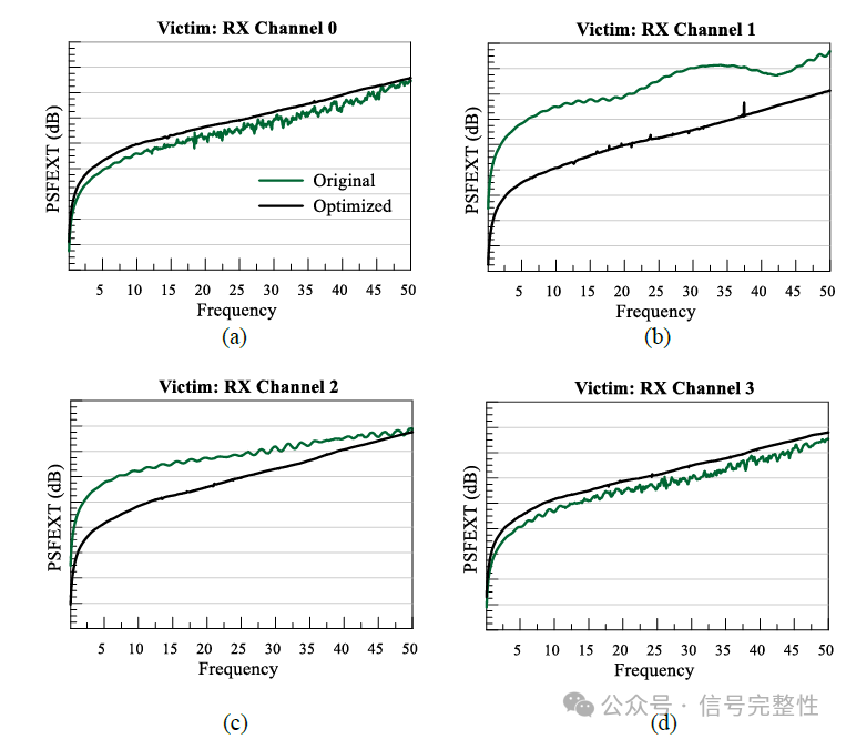
Fig. 8. Frequency domainsimulation results when victim is (a) RX ch0. (b)RX ch1. (c) RX ch2. and (d) RX ch3.
Table 2. Strongest of PSFEXT RX-RX below 14 and 28 GHz
B. Near-End Crosstalk of TX-RX
This section focuses onthe TX-RX near-end crosstalk. Fig. 9(a) and (b)show the PSNEXT TX-RX below 14 and 28 GHz, respectively, which are Nyquistfrequency for 56G and 112G PAM4. The x-axis represents the victim channelnumber, and the y-axis represents PSNEXT TX-RXin dB. The green, blue, and purplerepresent the PSNEXTTX- RX of Si interposer, package,and PCB, and the black one describesthe cascaded TX-RX. Fig. 9(c)-(f) show the simulatedS-parameter plots at different victim channel condition.
As shown in Fig. 9(a)and (b), the cascaded TX-RX is mainly limited due to both the packageand PCB. The main reason is thatthe package has a more dense and crowdeddesign at the C4 bump breakout area.In the following subsection, we analyze and optimizethe package TX-RX performance. In case of the channel0 and 3 in the PCB, the PSNEXTTX-RX are relatively higher than others becauseRX0 and RX3 are locatednear TX BGAs. Therefore, BGA pins should be re-arranged to mitigate inductive coupling, but it requires more BGAarea.
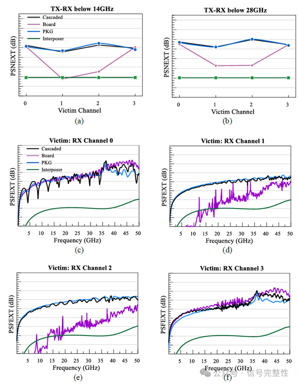
Fig. 9. PSNEXT TX-RX below (a) 14 and (b) 28 GHz.Simulated S-parameter plots when the victim is RX (c) ch0, (d)ch1, (e) ch2, and (f) ch3, respectively.
1)Package
The PSFEXT RX-RX and TX-TXcould be controlled well in the package design based on good BGA ballsarrangement, however, TX-RX has a stronger correlation with the design of theC4 bump area, including the arrangement of bumps and the integrity of the signalisolation. The C4 bump area is more complex with other vias of power domain orclock signal passing through.
Fig. 10 describes thevertical crosstalk mechanism due to vias within the crowded C4 bump breakout area. It assumesthat TX and RX tracesare formed on the nthand n+2th layers as a stripline, therefore solid ground planesare placed on then-1th, n+1th, andn+3th layers. However, due to designcomplexity, there could be vias including an anti-pad which can worsen TX-RX performance. Eventhough an electromagnetic field delivers energy with the self-ground from the differential mode, the via’s anti-padcan create an inevitablepath for energy to pass through depicted with the arrow in the above plot inthe Fig. 10. According to the theory [6], the distance between the via anti-padand traces should be three times larger than the trace width to perfectlyeliminate the vertical coupling, and/or the completed ground plane is neededbetween the TX and RX layers to isolate the EM field. However, in the advancedpackage design with a small form factor, it is hard to achieve them to routehigh-speed signal nets and meet design specifications.
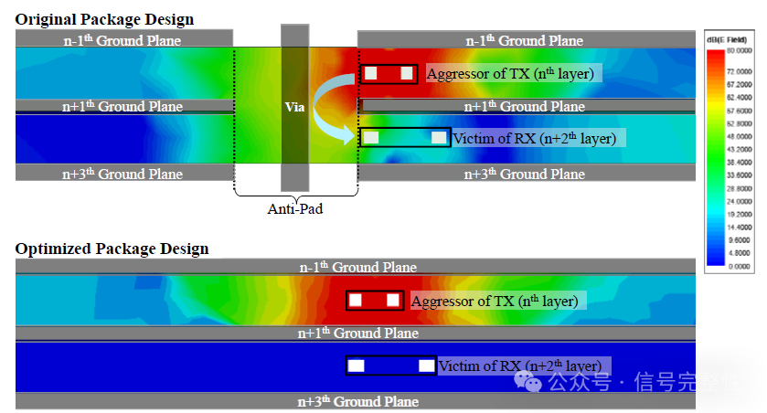
Fig. 10. Vertical couplingmechanism with EM field plots
Thus, we investigated twocase studies with different trace shapes and via-trace coupling near theC4 bump breakout area. In Fig. 11, the red line represents the RX signal on the n+2th layer,the blue line is the TX signal on the nth layer,and the green is the groundplane on the n+1th layer.For the case 1,the distance between the anti-padof vias from the RX signal nets is less than threetimes of trace width, and it has full via-trace coupling. Case 2 has fullvia-trace coupling as well as RX and TX traces are alsooverlapped which can cause thestronger vertical coupling effect.
As for the packagedesign optimization, we developed a golden templatewhere vias are located atleast three times of RX and TX trace width. Fig. 12(a) and (b) compare PSNEXT TX-RX between original and optimized package designs below 14 and 28 GHz which is Nyquist frequency for PAM4 56 Gbps and 112 Gbps, respectively. Also, Fig. 12 (c)-(f)show the detailed wave format. With the C4 breakout area optimization, thePSNEXT TX-RX is improved at both 14 GHzand 28 GHz. Especially, PSNEXT TX-RX at channel 2 is significantlyimproved about 54.2 % by increasingthe distance from trace to anti-pad to avoid vertical coupling. According tothe detail wave format, the sharp rise crosstalk noise around 35 GHz comes fromthe LC oscillation from the PTH structure.
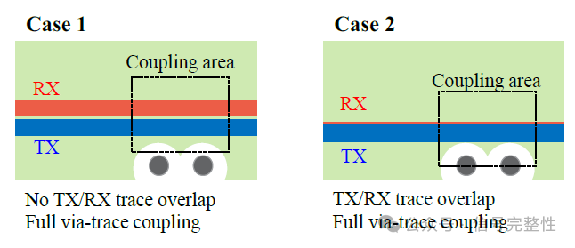
Fig. 11. Bump area optimized for channel 0 to channel3.
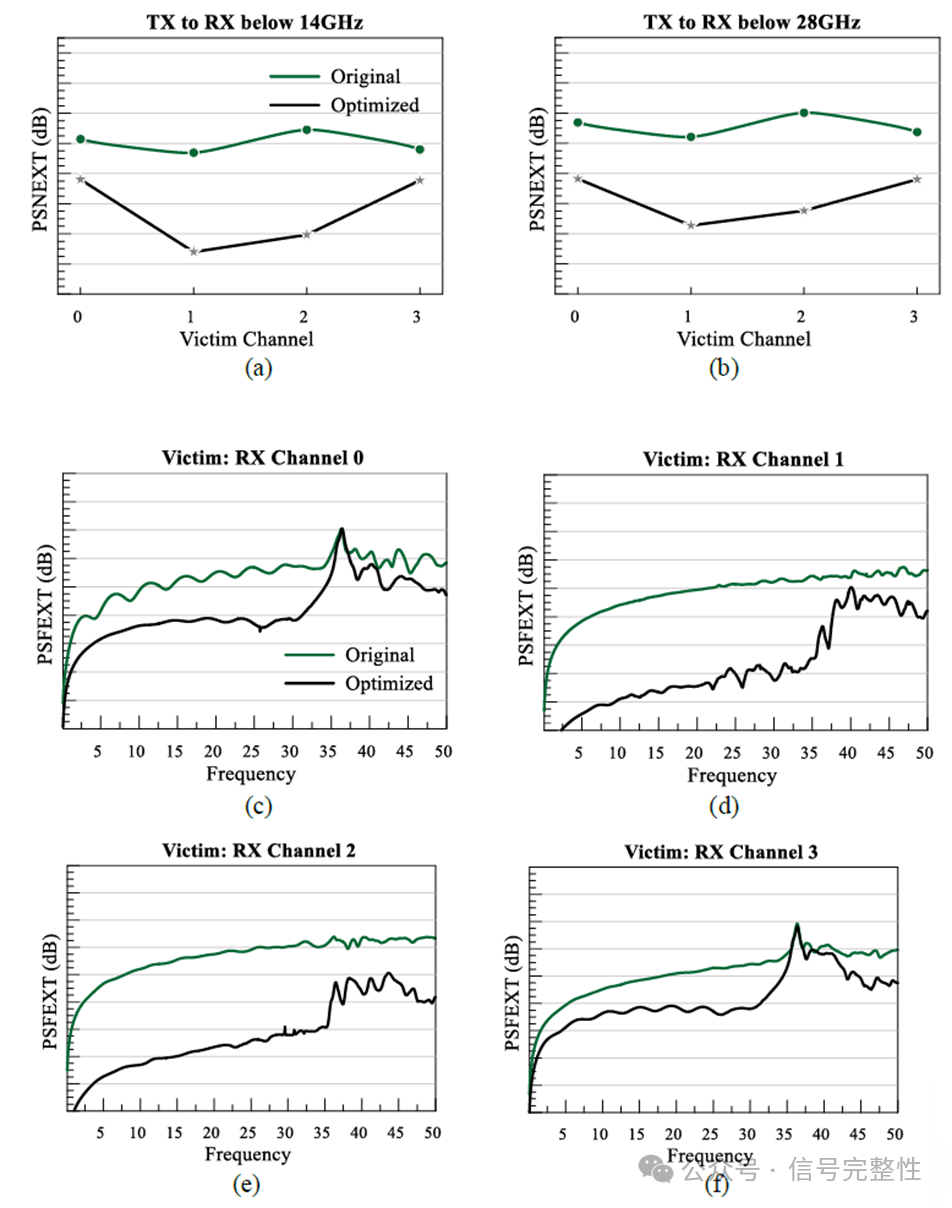
Fig. 12. TX-RX PSNEXT of the original and optimized design below (a) 14 GHz and (b) 28GHz. Simulated S-parameter plots when the victim channelis RX (c) ch0,(d)ch1, (e) ch2, and (f) ch3, respectively.
Although trace and viadesign rules can be checked using a script with a physical layout, 3D full-wavesimulation can provide more accurate estimation and prediction in frequencydomain so that the package can be signed off with high confidence. Fig. 13 comparesPSNEXT TX-RX on 35 SerDes channels between the original and optimized package designs.On average, there is 38 % improvement after optimizing the bumps area, andalso it showsa good standard deviation. The optimized designis stable and has minimal risk for the package design.
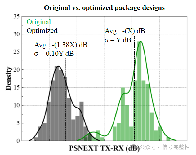
Fig. 13. PSNEXT TX-RX oforiginal and optimized packagedesign
Validation of 2.5D IC FPGA System Entire Channel in Frequency and Time Domain
In this section, we compare the FEXT/NEXT of the originaland optimized designs of the Si interposer, package,and PCB in both frequency and time domain. For transient simulation,system-level 112G PAM4 eye diagrams are compared.
A. Entire Channel Simulation in Frequency Domain
Fig. 14(a)-(c)compares PSFEXT RX-RXand TX-TX as well as PSNEXT TX-RX in the frequency domain between theoriginal and optimized designs with cascaded S- parameter of the Si interposer, package,and PCB. The green and black solidlines represent the originaland optimized designs. For this comparison, the case where channel 1 is thevictim is chosen among one SerDes quad.With the designoptimization of the Si interposer, package, and PCB as mentioned in the previoussections, the cascadedPSFEXT RX-RX is improved by about 24% below 28 GHz, also the PSNEXT TX-RX is enhancedabout 36% below 28 GHz compared to theoriginal design.
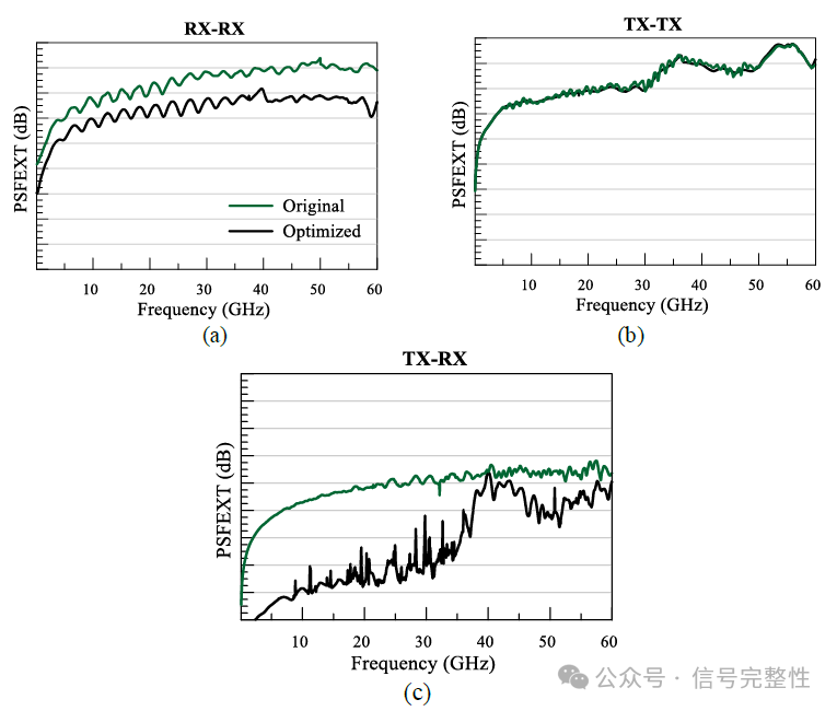
Fig. 14 PSFEXT (a) RX-RX (b) TX-TX and PSNEXT (c) TX-RX with original and optimized Si interposer, package, andPCB.
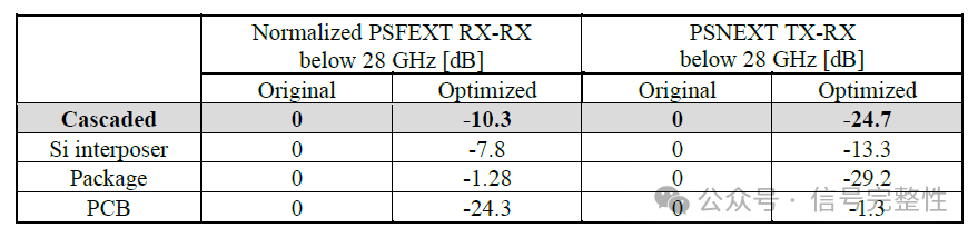
Fig. 15 illustrates thedetailed wave format of the original and optimized design. The green, blue,purple, and black lines in Fig. 15 show the crosstalk result with the Siinterposer, package, PCB, and the cascaded result, respectively, and Table 3summarizes the normalized worstcrosstalk performance below28 GHz. For the PSFEXTRX-RX, after increasing theRX-RX channel-to-channel distance as the TX-TX,PSFEXT RX-RX of Si interposer has gained 17 %. In addition, PCB crosstalk is significantlyenhanced about 59% after mitigating the vertical coupling effect by changing routinglayers.
For the PSFEXT TX-TX,the bottleneck exists in the PCB designdue to the signal traces routingon the relative deeper layers.Although there is no verticalcoupling effect in these different routing layers, thelength of the total vias to these deep layers will lead to stronger crosstalk. As the PSFEXT TX-TXis lower than the reference crosstalk of -50 dB in the original design, there is no other optimization item.
For the PSNEXT TX-RX,the package designbump area is optimized by increasingthe distance between the signaltraces and anti-padin order to mitigate the vertical coupling effect. With optimization, thechannel 1 is improved 43 % below 28 GHz.
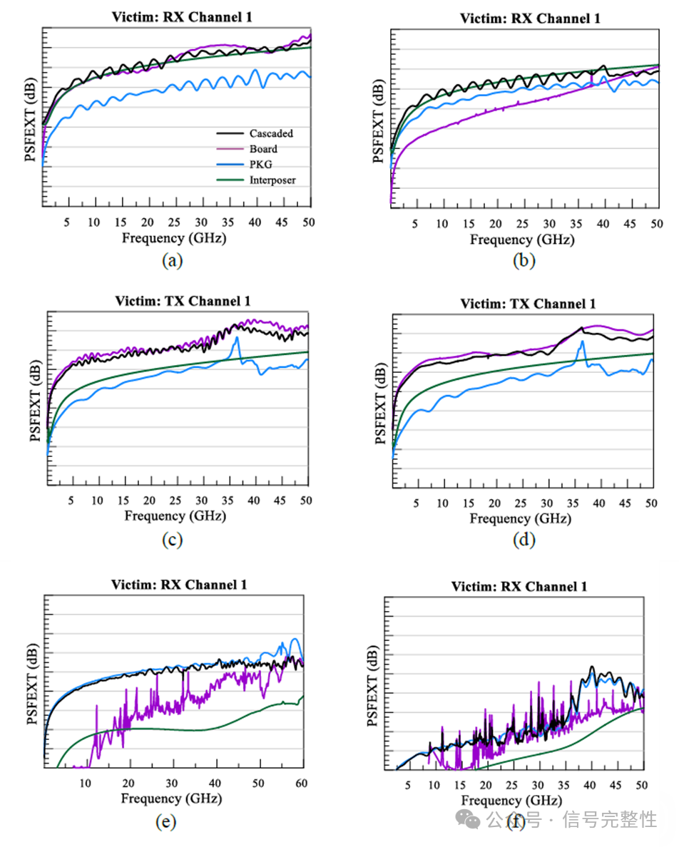
Fig. 15. PSFEXTRX-RX of (a) original (b) optimized design.PSFEXT TX-TX of (c) original(d) optimized design. PSNEXT TX-RX of (e) original (f) optimized design.
Table 3. Summaryof PSFEXT RX-RXand PSNEXT TX-RXbetween original and optimized designs.
B. Entire Channel Simulation in Time Domain
We also evaluate crosstalkoptimization in time domain with FPGA back-to-back links. As an example,112 Gbps PAM4 signal with 500 mVpp is generatedby the TX AMI model, and thenthe PAM4 signal is transmitted to the RX AMI model through the Si interposer, package,and PCB S-parameter model. The equalization parameters for TX/RX AMI models are optimized to support112 Gbps PAM4. To validate the crosstalk noise effect, we run channelsimulation without and with crosstalk noises based on the definition of RX-RX and TX-RX, and thenevaluate eye diagrams.
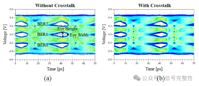
Fig. 16.Eye diagram of FEXTRX-RX. (a) With crosstalk noise.(b) Without crosstalk noise result in the originaldesign
Table 4. Summaryof eye height and width at different BER contours
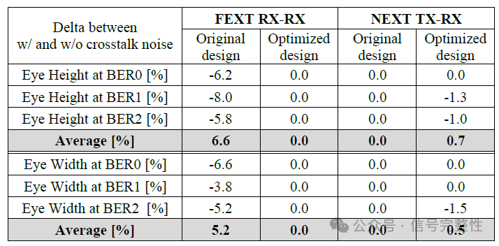
Fig. 16(a) and (b) showeye diagrams withoutand with RX-RX far-end crosstalk. Due to the crosstalk noises,eye-opening is degraded, and we summarized the eye height and width deltawithout and with RX-RX and TX-RX crosstalk for original and optimized designs, respectively. The FEXT RX-RXcolumn shows that the crosstalknoise affects 6.6% eye height and 5.2 % eye width degradation,respectively. However, the crosstalk has almost no influence on the optimizeddesign as Table 4. It clearly proves that the design shows excellent crosstalknoise reduction in time domain, in other words extremely low crosstalk noise level in frequency domain,and preserves good differential signalquality as well. For the caseof NEXT TX-RX, the crosstalk noise level is already lower than the FEXT RX-RXfor both originaland optimized designs,therefore, there is no big differencein terms of eye height and width in time-domain simulation.
Conclusion and Discussion
In this paper, we proposea co-design and co-simulation methodology for a 2.5D FPGA system to havehealthy and robust channel characteristics for the 112G PAM4 application. Inaddition, we clearly identified FEXT and NEXT and studied the crosstalk optimization methodsummarized below. The design methodology also includes a fast and effective physical verificationmethod to check the electrical performance of large-scale and advanced designsin both frequency and time domains. This method becomes invaluable as thedesign becomes complex and pursues high-speed in the next-generation deep nodeFPGA design. We believe that our crosstalk investigation can provide goodinsight to achieve a robust2.5D IC design, especially in helping to eliminate crosstalkrisk factors in the design stage.
Reference
[1]Karl Bois, et al., “System Design for 112G: Device characteristics, channel details and expected system performance,” DesignCon, 2021.
[2]Siow Chek Tan, etal., “Crosstalk and Switching Noise Mechanism Study in High DensityWire-bond FPGA Device,” InternationalElectronics Manufacturing Technology (IEMT) Conference, 2008.
[3]Hong Shi, etal., “Investigation of Package Crosstalk and Impact to 28-32GbpsTransceiver Jitter Margin,” IEEEElectronic Components and Technology Conference (ECTC), 2016.
[4]Daniel Wu, etal., “Crosstalk Associated with Solder Ball and/or Cutout-hole on thePower/Ground Planes/Nets,” IEEEInternational Symposium on Electromagnetic Compatibility (EMC), 2016.
[5] Xiaohong Jiang, et al., “Effective Die-Package-PCBCo-Design Methodology and its Deployment in 10 Gbps Serial Link Transceiver FPGA Packages,” InternationalMicrowave Symposium (IMS), 2009.
[6] S. H. Hall and H. L. Heck., “AdvancedSignal Integrity for High-Speed Digital Designs,” John Wiley & Sons, 2009.
[7] Po-Wei Chiu, et al., “Physical-Based Package Verification Methodology for High- SpeedChannel Crosstalk and Correlation with BERMeasurements,” IEEE Electronic Components and TechnologyConference (ECTC), submitted.
审核编辑:黄飞
-
PAM4 PRBS测试简介2025-01-15 3690
-
400G AOC产品的核心技术PAM4和DSP2019-03-19 4471
-
基于PAM4调制的400G光模块解析2021-02-20 5937
-
100G DWDM光模块中的PAM4与相干技术2021-03-04 3341
-
PAM4和NRZ信号的区别是什么2021-03-11 16001
-
本周推荐:关于200G PAM4光模块(推荐分享)2021-06-24 2464
-
问答专栏丨PAM4常见问题解答2021-06-28 3339
-
5G商用承载先行,50G PAM4白皮书发布2018-06-20 6668
-
Credo于TSMC 2018南京OIP研讨会首次公开展示7纳米工艺结点112G SerDes2018-10-30 6271
-
PAM4找到应用程序的一些方式及PAM4测试设置因应用程序而异2019-08-08 4837
-
112G PAM4 DAC如何实现机柜内布线2022-06-17 3334
-
400G QSFP112—助力IDC数据中心升级2023-10-20 2868
-
Samtec技术前沿 | 新型 Samtec前面板电缆系统带来112 Gbps PAM4优异性能2024-06-12 1058
-
AMD Versal自适应SoC GTM如何用XSIM仿真和观察PAM4信号2024-11-22 2186
-
全球首款4×112G 算力中心模拟CDR电芯片由上海米硅突破!2025-12-23 913
全部0条评论

快来发表一下你的评论吧 !
